

| Distributor | Stock | Pricing | MOQ | PKG | Lead Time | Date Code | On Order Quantity | On Order Delivery | |
|---|---|---|---|---|---|---|---|---|---|
|
8 pcs
|
8 pcs | On Request | 1 | On Request | On Request | On Request | On Request | On Request |
| Category | |
| Manufacturer Name | |
| Mounting Type | |
| Number of I | |
| Number of LABs | |
| Number of Logic Elements | |
| Operating Temperature | |
| SVHC Present | |
| Supplier Device Package | |
| Total RAM Bits | |
| Voltage |
The Intel 5CGXFC9A6U19I7 is a Field Programmable Gate Array (FPGA) from the Cyclone V GX series. It integrates 301,000 logic elements, 113,560 logic array blocks, and 14,251,008 bits of embedded memory, providing substantial resources for complex digital designs. The device offers 240 user I/O pins and operates over a supply voltage range of 1.07V to 1.13V. It is rated for junction temperatures from -40°C to 100°C, making it suitable for industrial and extended temperature environments.
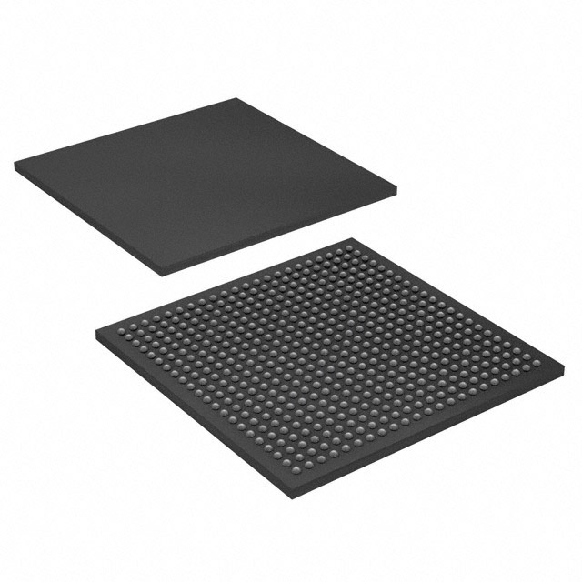
The FPGA is supplied in a 484-ball Fine-Pitch Ball Grid Array (FBGA) package, specifically the 484-UBGA (19x19 mm) variant, designed for surface mount assembly. The Cyclone V GX family is known for integrating transceivers and hard memory controllers, though specific transceiver counts are not confirmed in the available data. Intel provides comprehensive development support through the Quartus Prime software suite and a library of IP cores.
Typical applications include telecommunications infrastructure, industrial automation, consumer electronics, medical imaging, automotive advanced driver assistance systems, and aerospace/defense communications. The device is RoHS3 compliant and REACH unaffected, though these compliance statuses are unverified and should be confirmed with the manufacturer.
301000 logic elements.
240 I/O pins.
1.07V to 1.13V.
484-FBGA (484-UBGA 19x19 mm) surface-mount package.
14251008 bits (approximately 13.6 Mb).
-40°C to 100°C (junction temperature).
113560 logic array blocks.