

| Distributor | Stock | Pricing | MOQ | PKG | Lead Time | Date Code | On Order Quantity | On Order Delivery | |
|---|---|---|---|---|---|---|---|---|---|
|
6,000 pcs
|
6000 pcs | On Request | 1 | On Request | On Request | On Request | On Request | On Request |
| Category | |
| Manufacturer Name | |
| Mounting Type | |
| Number of I | |
| Number of LABs | |
| Number of Logic Elements | |
| Operating Temperature | |
| Supplier Device Package | |
| Termination Style | |
| Total RAM Bits | |
| Voltage |
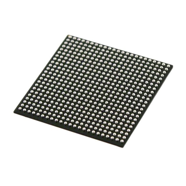
The Intel 5CGXFC3B7F23C8N is a Cyclone V FPGA designed for embedded applications requiring a balance of logic density and I/O capabilities. It features 31,500 logic elements (LEs) organized into 11,900 LABs/CLBs, providing ample resources for moderate complexity digital designs. The device includes 208 general-purpose I/O pins and 1,381,376 bits of total embedded RAM for data buffering and state storage.
This FPGA operates with a core supply voltage range of 1.07V to 1.13V, suitable for low-power applications. It is specified for commercial temperature range from 0°C to 85°C (TJ). The component is housed in a 484-ball BGA package with a supplier device package designation of 484-FBGA (23x23 mm), and is designed for surface mount assembly.
Typical applications include industrial control, communications infrastructure, and embedded processing where programmable logic is required. The device belongs to Intel's Cyclone V family, known for its balance of performance, power efficiency, and cost.
31500 logic elements.
208 user I/O pins.
1.07V to 1.13V.
484-BGA package with supplier device package 484-FBGA (23x23mm).
0°C to 85°C (TJ).
1381376 bits total RAM.
11900 LABs/CLBs.