

| Distributor | Stock | Pricing | MOQ | PKG | Lead Time | Date Code | On Order Quantity | On Order Delivery | |
|---|---|---|---|---|---|---|---|---|---|
|
3,250 pcs
|
3250 pcs | On Request | 1 | On Request | On Request | On Request | On Request | On Request |
| Category | |
| Manufacturer Name | |
| Mounting Type | |
| Number of I | |
| Number of LABs | |
| Number of Logic Elements | |
| Operating Temperature | |
| Supplier Device Package | |
| Total RAM Bits | |
| Voltage |
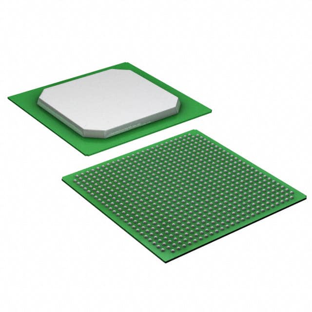
The 5CGTFD7D5F27I7N is a Field Programmable Gate Array (FPGA) from Intel's Cyclone V GT series. It integrates 149,500 logic elements and 56,480 logic array blocks (LABs), providing high logic density for complex digital designs. The device features 336 I/O pins and 7,880,704 bits of total RAM, enabling efficient data processing and storage.
The FPGA operates with a core supply voltage of 1.07V to 1.13V and supports an operating temperature range of -40°C to 100°C (junction). It is mounted using Surface Mount technology and is packaged in a 672-FBGA (27x27 mm) package. The device is compliant with RoHS3 and REACH, and is classified as MSL 3 (168 hours) for moisture sensitivity per the manufacturer page.
Designed for applications requiring high-speed logic and I/O, this FPGA is suitable for telecommunications, industrial automation, medical devices, consumer electronics, and military/aerospace systems. Intel's Quartus Prime software and IP cores support development and verification. The device also supports Error-Correcting Code (ECC) for data integrity, as noted in the manufacturer's description.
It has 149,500 logic elements.
The device provides 336 I/O pins.
The core supply voltage range is 1.07V to 1.13V.
It is packaged in a 672-FBGA (27x27 mm) package.
Total RAM bits are 7,880,704.
The operating junction temperature range is -40°C to 100°C.
The manufacturer page lists MSL 3 (168 hours). Note: database shows MSL 1; verify with datasheet.