

| Distributor | Stock | Pricing | MOQ | PKG | Lead Time | Date Code | On Order Quantity | On Order Delivery | |
|---|---|---|---|---|---|---|---|---|---|
|
60 pcs
|
60 pcs | On Request | 1 | On Request | On Request | On Request | On Request | On Request |
| Category | |
| Manufacturer Name | |
| Lead Style | |
| Mounting Type | |
| Number of I | |
| Number of LABs | |
| Number of Logic Elements | |
| Operating Temperature | |
| Supplier Device Package | |
| Total RAM Bits | |
| Voltage |
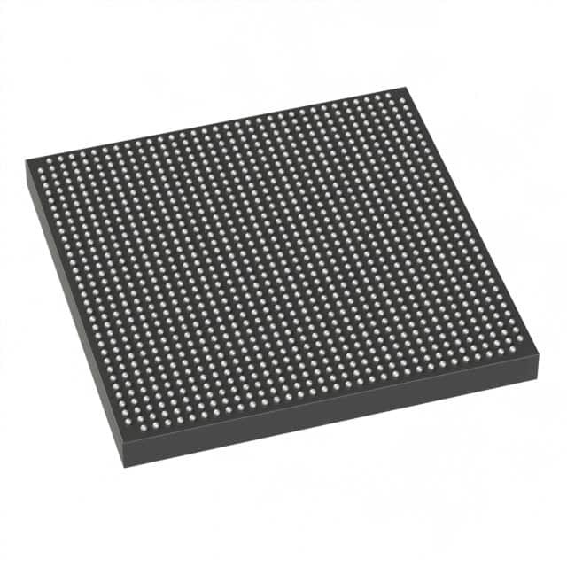
The Intel 5AGZME7H2F35I3LN is a field programmable gate array (FPGA) designed for high-density logic applications. It contains 450,000 logic elements organized into 21,225 logic array blocks (LABs), providing substantial digital logic capacity. The device integrates 40,249,344 bits of embedded RAM for on-chip data storage and features 534 user I/O pins for flexible peripheral interfacing.
The FPGA operates with a core supply voltage range of 0.82V to 0.88V, targeting low-power operation. It is specified for a junction temperature range of -40°C to 100°C, making it suitable for industrial and extended-temperature environments. The device is offered in a 1152-BBGA/FCBGA package with a 35x35 mm footprint and surface mount technology.
This component is intended for use in complex digital systems requiring high logic density, such as communications infrastructure, video processing, and industrial automation. The large number of I/O pins supports wide parallel buses, while the embedded memory reduces external component count. Proper thermal management is recommended for high-activity designs due to the package's power dissipation characteristics.
450,000 logic elements.
534 I/O pins.
0.82V to 0.88V.
1152-BBGA, FCBGA (1152-FBGA 35x35).
-40°C to 100°C (junction temperature).
40,249,344 bits (40.25 Mbit).
Surface Mount.