


| Distributor | Stock | Pricing | MOQ | PKG | Lead Time | Date Code | On Order Quantity | On Order Delivery | |
|---|---|---|---|---|---|---|---|---|---|
|
1 pcs
|
1 pcs | On Request | 1 | On Request | On Request | On Request | On Request | On Request |
| Category | |
| Manufacturer Name | |
| Mounting Type | |
| Number of I | |
| Number of LABs | |
| Number of Logic Elements | |
| Operating Temperature | |
| Supplier Device Package | |
| Total RAM Bits | |
| Voltage |
The Intel 5AGXFB7K4F40C5N is an Arria V GX Field Programmable Gate Array (FPGA) designed for high-performance digital applications. It features 504,000 logic elements, 23,780 logic array blocks (LABs), and 27,695,104 total RAM bits, providing substantial resources for complex logic designs.
This device offers 704 user I/O pins for extensive connectivity and operates from a supply voltage of 1.07V to 1.13V. It is specified for an operating temperature range of 0°C to 85°C (TJ), making it suitable for commercial temperature environments.
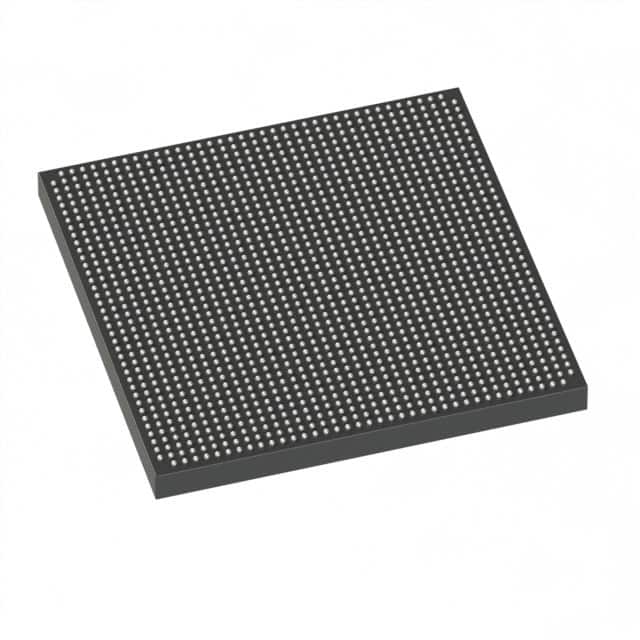
The FPGA is housed in a 1517-BBGA package with a supplier device package of 1517-FBGA (40x40 mm) and is designed for surface mount mounting. It is part of Intel's Arria V GX family, which balances logic density, memory, and I/O for applications such as wireless infrastructure, broadcast, and military communications.
The 5AGXFB7K4F40C5N has 504,000 logic elements.
The total RAM is 27,695,104 bits (27.7 Mbit).
The device provides 704 I/O pins.
The supply voltage range is 1.07V to 1.13V.
The operating temperature range is 0°C to 85°C (junction temperature).
It is available in a 1517-BBGA package, with a supplier device package of 1517-FBGA (40x40 mm).
The mounting type is Surface Mount.