

| Distributor | Stock | Pricing | MOQ | PKG | Lead Time | Date Code | On Order Quantity | On Order Delivery | |
|---|---|---|---|---|---|---|---|---|---|
|
2,505 pcs
|
2505 pcs | On Request | 1 | On Request | On Request | On Request | On Request | On Request |
| Category | |
| Manufacturer Name | |
| Mounting Type | |
| Number of I | |
| Number of LABs | |
| Number of Logic Elements | |
| Operating Temperature | |
| SVHC Present | |
| Supplier Device Package | |
| Termination Style | |
| Total RAM Bits | |
| Voltage |
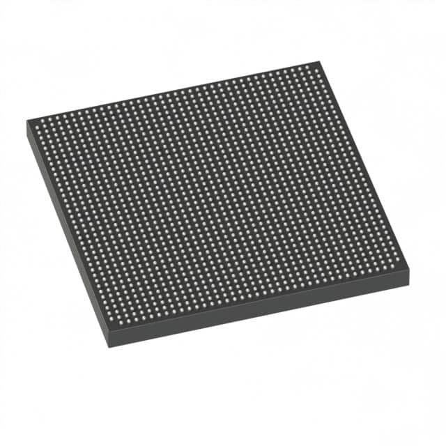
The Intel 5AGXFB3H4F40I5G is a Field Programmable Gate Array (FPGA) designed for high-performance embedded applications. It provides 362,000 logic elements and 17,110 LABs (Logic Array Blocks) for implementing complex digital logic. The device includes 19,822,592 bits of total RAM for on-chip data storage. With 704 user I/O pins, it offers extensive connectivity for interfacing with external peripherals and memory. The FPGA operates from a supply voltage range of 1.07V to 1.13V and is rated for an operating temperature range of -40°C to 100°C (junction). It is packaged in a 1517-BBGA, FCBGA (Flip Chip Ball Grid Array) package with a 40x40 mm footprint, suitable for surface mount assembly. The supplier device package is 1517-FBGA, FC (40x40). This FPGA is RoHS3 compliant and has a moisture sensitivity level of 1 (unlimited). It is commonly used in applications requiring high logic density and I/O count, such as communications, industrial control, and data processing.
362,000 logic elements.
704 I/O pins.
1.07V to 1.13V.
1517-FBGA, FC (40x40) surface mount package.
19,822,592 bits (19.8 Mbits).
-40°C to 100°C (junction).
17,110 LABs.