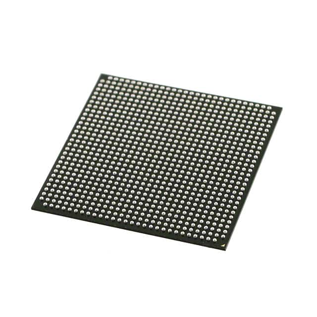
5AGXBB3D4F31C5N Intel 5AGXBB3D4F31C5N is an FPGA with 362000 logic elements, 384 I/O, and 19822592 bits RAM. It operates from 1.07V to 1.13V and is surface mount in 896-FBGA package.
Mfr Part #:

5AGXBB3D4F31C5N

Available from 1 distributors
Mfr Name: Intel
Intel
Intel 5AGXBB3D4F31C5N is an FPGA with 362000 logic elements, 384 I/O, and 19822592 bits RAM. It operates from 1.07V to 1.13V and is surface mount in 896-FBGA package.
Total Stock: 1,000 pcs

5AGXBB3D4F31C5N Available from 1 distributor

Authorised
Non-Authorised
Distributor Stock Pricing MOQ PKG Lead Time Date Code On Order Quantity On Order Delivery
Non-Authorised Inventory information
1,000 pcs
1000 pcs On Request 1 On Request On Request On Request On Request On Request

5AGXBB3D4F31C5N Specifications Quick View

Most important parameters for selection – full specs in datasheet.
Category
Manufacturer Name
Mounting Type
Number of I
Number of LABs
Number of Logic Elements
Operating Temperature
Supplier Device Package
Total RAM Bits
Voltage

5AGXBB3D4F31C5N Description

Short technical summary and product information.

The Intel 5AGXBB3D4F31C5N is a high-density Field Programmable Gate Array (FPGA) featuring 362,000 logic elements, 17,110 Logic Array Blocks (LABs), and 19,822,592 bits of embedded RAM. It provides 384 user I/O pins for flexible connectivity. The device operates from a core supply voltage of 1.07V to 1.13V and is specified for a temperature range of 0°C to 85°C. Housed in a 896-ball Fine-Pitch Ball Grid Array (FBGA) package measuring 31x31 mm, it is designed for surface mount assembly. This FPGA is suitable for complex digital logic designs requiring significant on-chip memory and high I/O count.

5AGXBB3D4F31C5N Quick Information

Product Type: FPGA (Field Programmable Gate Array)
Series: Arria V GX
Canonical Name: Intel 5AGXBB3D4F31C5N FPGA, 362000 Logic Elements, 384 I/O, 896-FBGA
Subcategory: Field Programmable Gate Array

5AGXBB3D4F31C5N Compliance

RoHS Status: RoHS Compliant
Moisture Sensitivity Level (MSL): 1 Unlimited
REACH Status: REACH Unaffected

5AGXBB3D4F31C5N Features

  • 362,000 logic elements for complex designs.
  • 19.8 Mbits of embedded RAM.
  • 384 user I/O pins for connectivity.
  • Surface mount 896-FBGA package.
  • 1.07V to 1.13V core supply voltage.

5AGXBB3D4F31C5N Applications

  • High-speed communications signal processing
  • Wireless baseband and infrastructure equipment
  • Video and image processing systems
  • Industrial automation and control
  • Defense and aerospace electronics

5AGXBB3D4F31C5N FAQs

7 frequently asked questions generated from this part’s specifications.
What is the number of logic elements?

362,000 logic elements.

How many I/O pins does this FPGA have?

384 I/O pins.

What is the supply voltage range?

1.07V to 1.13V.

What package is the 5AGXBB3D4F31C5N available in?

896-BBGA, FCBGA with supplier device package 896-FBGA (31x31).

How much embedded RAM does it have?

19,822,592 bits (approximately 19.8 Mbits).

What is the operating temperature range?

0°C to 85°C (TJ).

How many logic array blocks (LABs) are there?

17,110 LABs.

5AGXBB3D4F31C5N Alternate Parts

Same form/fit/function or matching attribute configuration across different manufacturers.
View All Alternate Parts
5AGXMB3G4F31C5N
5AGXMB3G4F31C5N
Intel
Intel FPGA featuring 362,000 logic elements, 384 I/O pins, 19.8 Mbit embedded RAM, in a 896-FBGA surface mount package.

View Part
Home
Account

Categories