
49FCT805SOG
Renesas
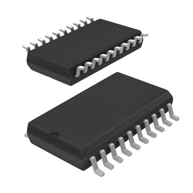
49FCT805SOG is a fanout buffer (distribution) IC from Renesas with a 1:5 input-to-output ratio, operating from 4.75V to 5.25V, in a 20-SOIC package.


| Distributor | Stock | Pricing | MOQ | PKG | Lead Time | Date Code | On Order Quantity | On Order Delivery | |
|---|---|---|---|---|---|---|---|---|---|
|
16,109 pcs
|
16109 pcs | On Request | 1 | On Request | On Request | On Request | On Request | On Request |
| Category | |
| Manufacturer Name | |
| Differential | |
| Input | |
| Mounting Type | |
| Number of Circuits | |
| Operating Temperature | |
| Output | |
| Ratio | |
| Supplier Device Package | |
| Type | |
| Voltage |
The 49FCT805SOG8 is a clock buffer and driver integrated circuit manufactured by Renesas Electronics Corporation. It is a fanout buffer (distribution) type device with a 1:5 input-to-output ratio, meaning it takes one clock input and provides five buffered outputs. The device contains two independent circuits.
The buffer accepts CMOS and LVTTL input logic levels and outputs CMOS and LVTTL signals. It does not support differential signaling. The supply voltage range is 4.75V to 5.25V. The operating temperature range is 0°C to 70°C.
The 49FCT805SOG8 is offered in a 20-SOIC surface mount package with a body width of 7.50mm. The supplier device package is also 20-SOIC. It is designed for surface mount assembly.
The supply voltage range is 4.75V to 5.25V.
The operating temperature range is 0°C to 70°C.
It comes in a 20-SOIC surface mount package with a body width of 7.50mm.
The input-to-output ratio is 1:5.
It supports CMOS and LVTTL logic levels for both input and output.
The manufacturer lists it as RoHS3 Compliant, but this is unverified.
It contains two independent buffer circuits.