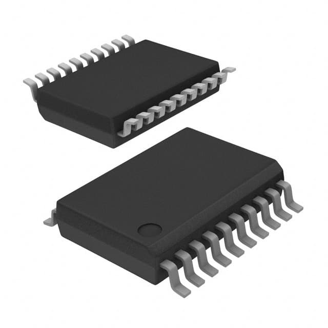
49FCT805PYG The Renesas 49FCT805PYG is a fanout clock buffer with a 1:5 ratio. It features CMOS/LVTTL inputs and outputs and is housed in a 20-SSOP package.
Mfr Part #:

49FCT805PYG

Available from 1 distributors
Mfr Name: Renesas
Renesas
The Renesas 49FCT805PYG is a fanout clock buffer with a 1:5 ratio. It features CMOS/LVTTL inputs and outputs and is housed in a 20-SSOP package.
Total Stock: 28,377 pcs

49FCT805PYG Available from 1 distributor

Authorised
Non-Authorised
Distributor Stock Pricing MOQ PKG Lead Time Date Code On Order Quantity On Order Delivery
Non-Authorised Inventory information
28,377 pcs
28377 pcs On Request 1 On Request On Request On Request On Request On Request

49FCT805PYG Specifications Quick View

Most important parameters for selection – full specs in datasheet.
Category
Manufacturer Name
Differential
Input
Mounting Type
Number of Circuits
Operating Temperature
Output
Ratio
Supplier Device Package
Type
Voltage

49FCT805PYG Description

Short technical summary and product information.

The Renesas 49FCT805PYG is a fanout buffer designed for clock distribution applications. It provides a 1:5 ratio, meaning one input signal can drive five output signals.


This device supports CMOS and LVTTL logic levels for both input and output signals, ensuring compatibility with a wide range of digital systems. It operates within a voltage range of 4.75V to 5.25V and is designed for surface mount installation.


The 49FCT805PYG is packaged in a 20-SSOP configuration, suitable for space-constrained PCB designs. It operates within a temperature range of 0°C to 70°C, making it suitable for various commercial and industrial applications.

49FCT805PYG Quick Information

Product Type: Clock Buffer
Canonical Name: Renesas 49FCT805PYG Clock Buffer
Subcategory: Clock Buffer

49FCT805PYG Compliance

RoHS Status: RoHS Compliant
Moisture Sensitivity Level (MSL): 1 Unlimited
REACH Status: REACH Unaffected

49FCT805PYG Features

  • Fanout buffer with 1:5 ratio.
  • CMOS and LVTTL input/output.
  • Operates from 4.75V to 5.25V.
  • Surface mount 20-SSOP package.
  • 0°C to 70°C operating temperature.

49FCT805PYG Applications

  • Distributes clock signals to multiple loads.
  • Buffers CMOS and LVTTL clock inputs.
  • Ideal for synchronous system timing distribution.
  • Provides 1:5 fanout for clock networks.
  • Used in digital logic clock buffering.

49FCT805PYG FAQs

5 frequently asked questions generated from this part’s specifications.
What is the supply voltage range of the 49FCT805PYG?

The supply voltage range is 4.75V to 5.25V.

What is the operating temperature range?

The operating temperature range is 0°C to 70°C.

What package is the 49FCT805PYG available in?

It is available in a 20-SSOP surface-mount package with a 5.30mm body width.

What input and output logic levels does the 49FCT805PYG support?

It supports CMOS and LVTTL logic levels for both input and output.

How many fanout circuits does the 49FCT805PYG have?

It has two fanout circuits, each with a 1:5 ratio.

49FCT805PYG Alternate Parts

Same form/fit/function or matching attribute configuration across different manufacturers.
View All Alternate Parts
49FCT805PYG8
49FCT805PYG8
Renesas
49FCT805PYG8 is a fanout buffer (distribution) IC from Renesas with a 1:5 input-to-output ratio, operating from 4.75V to 5.25V, in a 20-SSOP package.

View Part
49FCT805APYG
49FCT805APYG
Renesas
IC CLK BUFFER 1:5 20SSOP
View Part
IDT49FCT805APY8
IDT49FCT805APY8
Renesas
IC CLK BUFFER 1:5 20SSOP
View Part
IDT49FCT805APY
IDT49FCT805APY
Renesas
IC CLK BUFFER 1:5 20SSOP
View Part
Home
Account

Categories