


| Distributor | Stock | Pricing | MOQ | PKG | Lead Time | Date Code | On Order Quantity | On Order Delivery | |
|---|---|---|---|---|---|---|---|---|---|
|
10,884 pcs
|
10884 pcs | On Request | 1 | On Request | On Request | On Request | On Request | On Request |
| Category | |
| Manufacturer Name | |
| Differential | |
| Input | |
| Mounting Type | |
| Number of Circuits | |
| Operating Temperature | |
| Output | |
| Ratio | |
| Supplier Device Package | |
| Type | |
| Voltage |
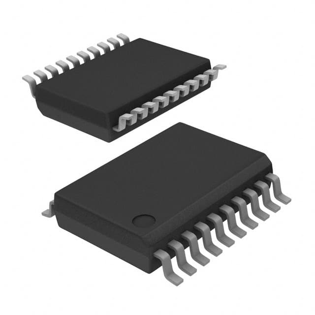
The Renesas 49FCT805BTPYG8 is a clock buffer and driver IC designed for efficient clock signal distribution. It offers a 1:5 fanout ratio, allowing a single input clock signal to drive multiple outputs. The device supports both CMOS and LVTTL logic levels for input and output signals, providing flexibility in system integration.
With an operating voltage range of 4.5V to 5.5V and an operating temperature range of 0°C to 70°C, this buffer is suitable for various commercial applications. It is housed in a 20-SSOP surface mount package, measuring 0.209 inches (5.30mm) in width, which is ideal for space-constrained PCB designs.
The buffer is configured with 2 independent circuits, each providing clock distribution. Its RoHS3 compliant status and Moisture Sensitivity Level 1 rating indicate adherence to environmental standards and ease of handling during manufacturing.
The fanout ratio is 1:5.
It supports CMOS and LVTTL input and output.
The operating voltage range is 4.5V to 5.5V.
The operating temperature range is 0°C to 70°C.
The device is available in a 20-SSOP surface mount package (0.209", 5.30mm width).
The device contains two buffer circuits.
No, the buffer is not differential; both input and output are single-ended.