

| Distributor | Stock | Pricing | MOQ | PKG | Lead Time | Date Code | On Order Quantity | On Order Delivery | |
|---|---|---|---|---|---|---|---|---|---|
|
4,512 pcs
|
4512 pcs | On Request | 1 | On Request | On Request | On Request | On Request | On Request |
| Category | |
| Manufacturer Name | |
| Current | |
| Drain to Source Voltage (Vdss) | |
| Drive Voltage (Max Rds On, Min Rds On) | |
| FET Type | |
| Gate Charge (Qg) (Max) @ Vgs | |
| Halogen Free | |
| Input Capacitance (Ciss) (Max) @ Vds | |
| Mounting Type | |
| Operating Temperature | |
| Power Dissipation (Max) | |
| Rds On (Max) @ Id, Vgs | |
| Storage Temperature | |
| Supplier Device Package | |
| Tape & Reel | |
| Technology | |
| Vgs (Max) |
The 3LP01C-TB-H is a P-Channel small signal MOSFET designed by ON Semiconductor. It offers a maximum drain-source voltage of -30V and a continuous drain current of -0.1A, making it suitable for low-power load switching and signal processing applications. The device features a low on-resistance of 10.4Ω at 4V gate drive, which minimizes conduction losses.
This MOSFET supports 2.5V and 1.5V gate drive voltages, enabling operation with low-voltage logic. Its high-speed switching characteristics, with typical rise and fall times of 55ns and 130ns respectively, allow efficient performance in switching circuits. The gate charge is only 1.43nC, further reducing drive requirements.
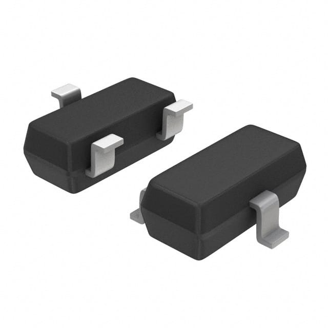
The device is housed in a surface-mount SC-59-3 package (also known as SOT-23-3 or TO-236-3), which is ideal for compact PCB layouts. It is available in tape and reel packaging with 3,000 pieces per reel. The -TB-H variant is lead-free and halogen-free, meeting environmental standards.
| Qty | Low | High |
|---|---|---|
| 2,597+ | $0.12 | $0.12 |
Estimated market price range - modelled values for guidance only, not live distributor offers.
The maximum drain-source voltage is -30V.
The device is available in a surface-mount SC-59-3 package (also compatible with SOT-23-3 and TO-236-3).
The maximum channel temperature is 150°C, with a storage temperature range of -55°C to +150°C.
RoHS3 Compliant (unverified). The -TB-H variant is confirmed lead-free and halogen-free per the datasheet.
The maximum continuous drain current is -0.1A, with a pulse current rating of -0.4A.
The typical total gate charge is 1.43nC at Vgs=-10V, with gate-source charge 0.18nC and gate-drain charge 0.25nC.
Typical switching times: turn-on delay 24ns, rise time 55ns, turn-off delay 120ns, fall time 130ns.