

| Distributor | Stock | Pricing | MOQ | PKG | Lead Time | Date Code | On Order Quantity | On Order Delivery | |
|---|---|---|---|---|---|---|---|---|---|
|
63,000 pcs
|
63000 pcs | On Request | 1 | On Request | On Request | On Request | On Request | On Request |
| Category | |
| Manufacturer Name | |
| Current | |
| Drain to Source Voltage (Vdss) | |
| Drive Voltage (Max Rds On, Min Rds On) | |
| FET Type | |
| Gate Charge (Qg) (Max) @ Vgs | |
| Input Capacitance (Ciss) (Max) @ Vds | |
| Mounting Type | |
| Operating Temperature | |
| Power Dissipation (Max) | |
| Rds On (Max) @ Id, Vgs | |
| Storage Temperature | |
| Supplier Device Package | |
| Tape & Reel | |
| Technology | |
| Vgs (Max) |
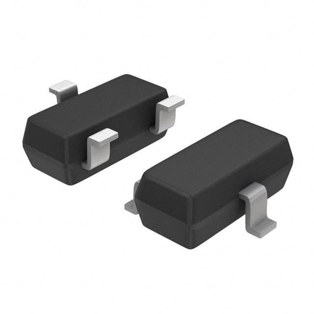
The 3LN01C-TB-E is an N-Channel small signal MOSFET from ON Semiconductor designed for low-power switching applications. It features a drain-source breakdown voltage of 30V and a continuous drain current of 150mA at 25°C ambient temperature. The device offers low on-resistance of 3.7Ω maximum at 4V gate drive, enabling efficient switching with minimal conduction losses. With a gate threshold voltage range of 0.4V to 1.3V, it can be driven by low-voltage logic signals as low as 1.5V. The MOSFET is housed in a surface-mount SC-59 (TO-236, SOT-23-3) package, making it suitable for compact PCB designs. It is supplied in tape and reel packaging with 3000 pieces per reel. The device is Pb-free and designed for ESD immunity below 200V (Machine Model). Typical applications include load switching, DC-DC converters, and signal switching in portable electronics.
30V minimum at ID=1mA, VGS=0V.
150mA maximum at Ta=25°C.
3.7Ω maximum at VGS=4V, ID=80mA; 5.2Ω maximum at VGS=2.5V, ID=40mA.
0.4V minimum to 1.3V maximum at VDS=10V, ID=100μA.
Channel temperature maximum 150°C; storage temperature range -55 to +150°C.
SC-59, TO-236, SOT-23-3 (surface mount).
RoHS3 Compliant (unverified). The datasheet confirms Pb-free finish.