

| Distributor | Stock | Pricing | MOQ | PKG | Lead Time | Date Code | On Order Quantity | On Order Delivery | |
|---|---|---|---|---|---|---|---|---|---|
|
68,865 pcs
|
68865 pcs | On Request | 1 | On Request | On Request | On Request | On Request | On Request |
| Category | |
| Manufacturer Name | |
| Current | |
| Current Drain (Id) | |
| Drain to Source Voltage (Vdss) | |
| FET Type | |
| Mounting Type | |
| Operating Temperature | |
| Power | |
| Storage Temperature | |
| Supplier Device Package | |
| Tape & Reel | |
| Voltage |
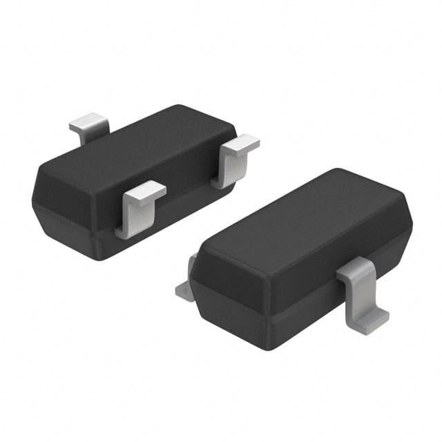
The 2SK932-23-TB-E is an N-Channel JFET manufactured by On Semiconductor, designed for RF amplification and low-noise applications. It utilizes the FBET process to achieve low noise figure and high forward transfer admittance. Key electrical specifications include a maximum drain-to-source voltage of 15 V, drain current of 50 mA, and power dissipation of 200 mW. The device features a zero-gate voltage drain current range of 10.0 to 24.0 mA and a cutoff voltage between -0.2 and -1.4 V. With a typical input capacitance of 10 pF and reverse transfer capacitance of 3 pF, it is suitable for high-frequency circuits. The JFET is offered in a surface-mount SMCP package, compatible with SC-59, SOT-23-3, and TO-236-3 footprints. It is supplied in tape and reel packaging with 3000 units per reel. The device is Pb-Free and RoHS compliant.
Typical applications include AM tuner RF amplification and low-noise amplifier stages. The low noise figure of 1.5 dB at 1 kHz makes it ideal for sensitive signal processing. The device is rated for junction temperatures up to 150°C and storage from -55°C to 150°C.
| Qty | Low | High |
|---|---|---|
| 1+ | $0.70 | $0.70 |
| 10+ | $0.43 | $0.43 |
| 50+ | $0.32 | $0.32 |
| 100+ | $0.28 | $0.28 |
| 500+ | $0.21 | $0.21 |
| 3,000+ | $0.15 | $0.15 |
| 6,000+ | $0.13 | $0.13 |
| 9,000+ | $0.08 | $0.08 |
Estimated market price range - modelled values for guidance only, not live distributor offers.
15 V.
Maximum junction temperature is 150°C, storage temperature range -55 to +150°C.
Surface-mount SMCP package, compatible with SC-59, SOT-23-3, and TO-236-3.
The datasheet states it is Pb-Free, and the RoHS status is listed as RoHS3 compliant (unverified).
1.5 dB at 1 kHz.
10 pF typical.
Rank 23: 10.0 to 17.0 mA; Rank 24: 14.5 to 24.0 mA.