

| Distributor | Stock | Pricing | MOQ | PKG | Lead Time | Date Code | On Order Quantity | On Order Delivery | |
|---|---|---|---|---|---|---|---|---|---|
|
4 pcs
|
4 pcs | On Request | 1 | On Request | On Request | On Request | On Request | On Request |
| Category | |
| Manufacturer Name | |
| Lead Spacing | |
| Lead Style | |
| Mounting Type | |
| Storage Temperature | |
| Tape & Reel | |
| Termination Style |
The Continental Device India Ltd (CDIL) 2N5322 is an NPN silicon power switching transistor. It is designed for medium power amplifier and switching applications.
Key electrical characteristics include a continuous collector current (IC) of 2.1A and a collector-emitter voltage (VCEO) of 75V. The transistor features a DC current gain (hFE) ranging from 30 to 160 at IC=0.5A, VCE=4V. Its turn-on time is a maximum of 100ns and turn-off time is a maximum of 1000ns under specified test conditions.
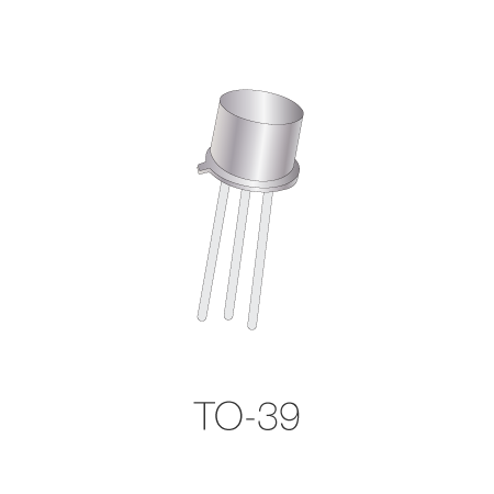
The device is housed in a TO-39 metal can package, suitable for through-hole mounting. Thermal characteristics include a junction-to-case thermal resistance (Rth(j-c)) of 17.5 °C/W, allowing for efficient heat dissipation when properly mounted.
This transistor operates within a junction temperature range of -65°C to +200°C.
| Qty | Low | High |
|---|---|---|
| 1+ | $0.77 | $0.77 |
Estimated market price range - modelled values for guidance only, not live distributor offers.
The maximum collector-emitter voltage (VCEO) for the 2N5322 is 75V.
The continuous collector current (IC) for the 2N5322 is 2.1A.
The 2N5322 transistor is supplied in a TO-39 metal can package.
The operating junction temperature range for the 2N5322 is -65°C to +200°C.
The DC current gain (hFE) for the 2N5322 at IC=0.5A, VCE=4V ranges from 30 to 160.
The turn-on time (ton) for the 2N5322 is a maximum of 100ns, and the turn-off time (toff) is a maximum of 1000ns under specified conditions.