

| Distributor | Stock | Pricing | MOQ | PKG | Lead Time | Date Code | On Order Quantity | On Order Delivery | |
|---|---|---|---|---|---|---|---|---|---|
|
5,750 pcs
|
5750 pcs | On Request | 1 | On Request | On Request | On Request | On Request | On Request |
| Category | |
| Manufacturer Name | |
| Drain to Source Voltage (Vdss) | |
| FET Type | |
| Input Capacitance (Ciss) (Max) @ Vds | |
| Mounting Type | |
| Power | |
| Resistance | |
| Storage Temperature | |
| Supplier Device Package | |
| Tape & Reel | |
| Turn Off Time | |
| Turn On Time | |
| Voltage |
The 2N5116 is a silicon P-Channel JFET designed for switching applications. It features a maximum drain-source voltage of 30V, gate-source voltage of 30V, and gate current of 50mA. Power dissipation is rated at 500mW, with an operating and storage junction temperature range of -65°C to 200°C.
Electrical characteristics include a drain current (IDSS) of 5.0 mA to 25 mA at VDS=15V, gate-source cutoff voltage of 1.0V to 4.0V, and maximum drain-source on-resistance of 150Ω. Input capacitance is 25pF maximum, and reverse transfer capacitance is 7.0pF maximum. Switching times are 42ns turn-on and 60ns turn-off under specified test conditions.
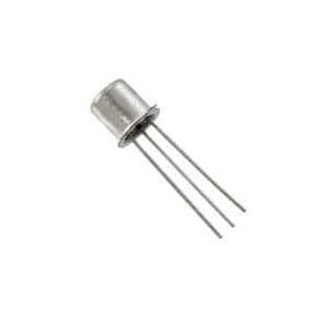
The device is housed in a TO-206AA / TO-18-3 metal can package with through-hole mounting. Lead configuration is Source, Gate, Drain. This JFET is suitable for low-power analog switching and signal gating applications.
The maximum drain-source voltage (VDS) is 30V.
The 2N5116 is available in a TO-206AA / TO-18-3 metal can through-hole package (supplier device package TO-18).
The operating and storage junction temperature range is -65°C to 200°C.
The 2N5116 is listed as RoHS3 Compliant, but this information is unverified and has low confidence.
The drain current (IDSS) at VDS=15V ranges from 5.0 mA to 25 mA.
The maximum drain-source on-resistance (rDS(ON)) is 150Ω at ID=1mA, VGS=0.
Turn-on time is 42 ns maximum and turn-off time is 60 ns maximum under specified test conditions.