

| Distributor | Stock | Pricing | MOQ | PKG | Lead Time | Date Code | On Order Quantity | On Order Delivery | |
|---|---|---|---|---|---|---|---|---|---|
|
2,524 pcs
|
2524 pcs | On Request | 1 | On Request | On Request | On Request | On Request | On Request |
| Category | |
| Manufacturer Name | |
| Configuration | |
| Input Capacitance | |
| Mounting Type | |
| Power Dissipation | |
| Storage Temperature | |
| Supplier Device Package | |
| Tape & Reel | |
| Technology | |
| Voltage |
The 2N3819 is a silicon N-Channel JFET designed for RF amplifier and mixer applications. It has a maximum drain-source voltage of 25V and a maximum continuous gate current of 10mA. The device features a drain-source saturation current (IDSS) range of 2.0 to 20mA at VDS=15V, and a gate-source cutoff voltage (VGS(OFF)) of up to 8.0V. Forward transconductance (|Yfs|) is 2.0 to 6.5mS at 1.0MHz and a minimum of 1.6mS at 100MHz. Input capacitance (Ciss) is a maximum of 8.0pF and reverse transfer capacitance (Crss) is a maximum of 4.0pF.
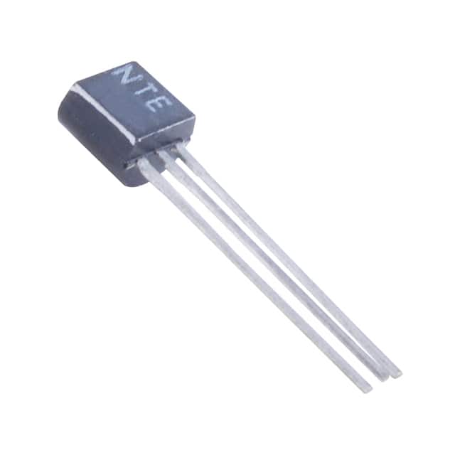
The device is housed in a through-hole TO-92 package (TO-226-3, TO-92-3) with a lead code of drain, gate, source. The operating and storage junction temperature range is -65°C to +150°C. This JFET is well-suited for low-noise RF amplifier and mixer circuits in applications such as radios, communications equipment, and test instrumentation.
The maximum drain-source voltage is 25 V.
The 2N3819 is available in a through-hole TO-92 package (TO-226-3, TO-92-3).
The operating and storage junction temperature range is -65°C to +150°C.
The maximum power dissipation is 360 mW.
The maximum gate-source cutoff voltage is 8.0 V at VDS=15V and ID=2.0nA.
The maximum input capacitance is 8.0 pF at VDS=15V, VGS=0, and f=1.0MHz.
RoHS status is listed as RoHS3 Compliant, but this is unverified.