

| Distributor | Stock | Pricing | MOQ | PKG | Lead Time | Date Code | On Order Quantity | On Order Delivery | |
|---|---|---|---|---|---|---|---|---|---|
|
1,340 pcs
|
1340 pcs | On Request | 1 | On Request | On Request | On Request | On Request | On Request |
| Category | |
| Manufacturer Name | |
| Current | |
| Halogen Free | |
| Mounting Type | |
| Propagation Delay | |
| Tape & Reel | |
| Voltage |
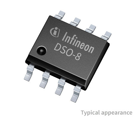
The Infineon 2ED2181S06F is a high-voltage, high-speed power MOSFET and IGBT driver. It offers independent high and low side referenced output channels, based on Infineon's SOI-technology for excellent ruggedness and noise immunity.
Key electrical specifications include a maximum VS_OFFSET of 650V, typical output peak current of +/- 2.5A, and operating voltages (VS node) up to +650V. The device supports bootstrap operation with a maximum bootstrap voltage (VB node) of +675V. It features delay matching of 35ns max and a propagation delay of 200ns. The driver is compatible with 3.3V, 5V, and 15V logic inputs and can operate at negative voltages down to -11V on the VS pin.
Potential applications for the 2ED2181S06F include driving IGBTs and enhancement mode N-Channel MOSFETs in various power electronic applications such as motor drives, general-purpose inverters, refrigeration compressors, induction cookers, and offline AC-DC power supplies. It is available in DSO-8 and DSO-14 package options.
The device is RoHS compliant and has a Moisture Sensitivity Level (MSL) of 1.
| Qty | Low | High |
|---|---|---|
| 1+ | $2.01 | $2.01 |
Estimated market price range - modelled values for guidance only, not live distributor offers.
The maximum operating voltage for the VS node is 650 V.
The typical output current (Io+pk / Io-pk) is + 2.5 A/ - 2.5 A.
The delay matching is a maximum of 35 ns.
The 2ED2181S06F is available in DSO-8 and DSO-14 package options.
The product is listed as RoHS3 Compliant.