

| Distributor | Stock | Pricing | MOQ | PKG | Lead Time | Date Code | On Order Quantity | On Order Delivery | |
|---|---|---|---|---|---|---|---|---|---|
|
95 pcs
|
95 pcs | On Request | 1 | On Request | On Request | On Request | On Request | On Request | |
|
95 pcs
|
95 pcs | On Request | 1 | On Request | On Request | On Request | On Request | On Request | |
|
1 pcs
|
1 pcs | On Request | 1 | On Request | On Request | On Request | On Request | On Request |
| Category | |
| Manufacturer Name | |
| Differential | |
| Divider | |
| Frequency | |
| Input | |
| Lead Style | |
| Mounting Type | |
| Number of Circuits | |
| Operating Temperature | |
| Output | |
| PLL | |
| Ratio | |
| Supplier Device Package | |
| Type | |
| Voltage |
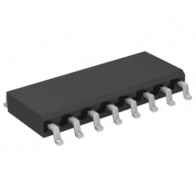
The 2308-2DCGI8 is a clock multiplier and zero delay buffer integrated circuit from Renesas. It accepts a single LVTTL input and provides eight LVTTL outputs with a 1:8 ratio. The device includes a PLL with bypass capability and operates at frequencies up to 133.3 MHz. It is designed for clock distribution in digital systems requiring low skew and zero delay. The IC operates from a 3V to 3.6V supply and is specified over the industrial temperature range of -40°C to 85°C. It is housed in a 16-pin SOIC package (16-SOIC, 0.154" width, 3.90mm body) and is surface mountable. This component is suitable for applications such as memory clocking, networking, and computing where precise clock multiplication and distribution are needed.
3V to 3.6V.
16-SOIC (0.154", 3.90mm Width) surface mount package.
-40°C to 85°C.
RoHS3 Compliant (unverified).
133.3 MHz.
LVTTL for both input and output.
8 outputs (1:8 input-to-output ratio).