

| Distributor | Stock | Pricing | MOQ | PKG | Lead Time | Date Code | On Order Quantity | On Order Delivery | |
|---|---|---|---|---|---|---|---|---|---|
|
4,772 pcs
|
4772 pcs | On Request | 1 | On Request | On Request | On Request | On Request | On Request |
| Category | |
| Manufacturer Name | |
| Differential | |
| Divider | |
| Frequency | |
| Input | |
| Mounting Type | |
| Number of Circuits | |
| Operating Temperature | |
| Output | |
| PLL | |
| Ratio | |
| Supplier Device Package | |
| Type | |
| Voltage |
The 2308-1HPGGI is a clock multiplier and zero delay buffer integrated circuit from Renesas. It is designed to generate multiple synchronized clock outputs from a single input, making it suitable for clock distribution in digital systems.
This device features a 1:8 input-to-output ratio, allowing one LVTTL input to drive eight LVTTL outputs. It includes a Phase-Locked Loop (PLL) with bypass capability, and operates at a maximum frequency of 133.3 MHz. The supply voltage range is 3V to 3.6V.
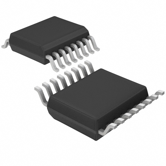
The 2308-1HPGGI is housed in a 16-TSSOP surface mount package with a 4.40mm width. It is rated for an operating temperature range of -40°C to 85°C, making it suitable for industrial environments.
The maximum frequency is 133.3 MHz.
The input-to-output ratio is 1:8.
Both the input and output use LVTTL logic levels.
The supply voltage range is 3V to 3.6V.
It comes in a 16-TSSOP surface mount package with a 4.40mm width.
The operating temperature range is -40°C to 85°C.
Yes, it has a PLL with bypass capability.