

| Distributor | Stock | Pricing | MOQ | PKG | Lead Time | Date Code | On Order Quantity | On Order Delivery | |
|---|---|---|---|---|---|---|---|---|---|
|
7,399 pcs
|
7399 pcs | On Request | 1 | On Request | On Request | 18+ | On Request | On Request | |
|
1,623 pcs
|
1623 pcs | On Request | 1 | On Request | On Request | On Request | On Request | On Request | |
|
780 pcs
|
780 pcs | On Request | 1 | On Request | On Request | 22+ | On Request | On Request | |
|
28 pcs
|
28 pcs | On Request | 1 | On Request | On Request | On Request | On Request | On Request |
| Category | |
| Manufacturer Name | |
| Current | |
| Latch-up Performance | |
| Logic Type | |
| Mounting Type | |
| Number of Bits per Element | |
| Number of Elements | |
| Operating Temperature | |
| Output Type | |
| Supplier Device Package | |
| Voltage | |
| Voltage Supply |
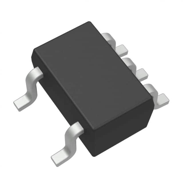
This Texas Instruments 1P1G125QDCKRQ1 is a single, non-inverting buffer gate designed for 1.65V to 5.5V VCC operation. It features a 3-state output that is disabled when the output-enable input is high.
The device offers high output drive of ±24mA at 3.3V while maintaining low static power dissipation. It supports a broad VCC operating range and has an ambient operating temperature range of -40°C to 125°C.
Key electrical characteristics include a maximum propagation delay of 3.7 ns at 3.3V and low power consumption with a maximum I CC of 10 μA. The buffer gate is AEC-Q100 qualified, indicating its suitability for automotive applications.
Packaged in a compact SC-70-5 surface-mount package, this component is suitable for designs where space is a constraint. Its over-voltage tolerant inputs accept voltages up to 5.5V, providing design flexibility.
| Qty | Low | High |
|---|---|---|
| 1+ | $1.20 | $1.20 |
Estimated market price range - modelled values for guidance only, not live distributor offers.
The device operates from 1.65V to 5.5V.
-40°C to 125°C ambient operating temperature.
Surface-mount SC-70-5 (also known as SOT-353).
±24 mA at 3.3V.
3.7 ns maximum at 3.3V.
10 μA maximum.
HBM Level 2, CDM Level C5.