

| Distributor | Stock | Pricing | MOQ | PKG | Lead Time | Date Code | On Order Quantity | On Order Delivery | |
|---|---|---|---|---|---|---|---|---|---|
|
1,149 pcs
|
1149 pcs | On Request | 1 | On Request | On Request | On Request | On Request | On Request |
| Category | |
| Manufacturer Name | |
| Mounting Type | |
| Number of I | |
| Number of LABs | |
| Number of Logic Elements | |
| Operating Temperature | |
| Supplier Device Package | |
| Total RAM Bits | |
| Voltage |
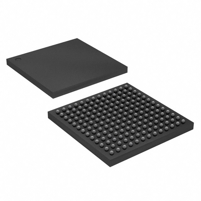
The 10M16SCU169I7G is a Field Programmable Gate Array (FPGA) from Intel. It contains 16,000 logic elements arranged in 1,000 Logic Array Blocks (LABs), providing flexible digital logic implementation for a wide range of embedded applications. The device offers 130 user I/O pins and 562,176 bits of total RAM, enabling moderate complexity designs with on-chip memory.
The FPGA operates with a supply voltage ranging from 2.85V to 3.465V and is rated for a junction temperature range of -40°C to 100°C. It is housed in a 169-LFBGA (Low-profile Fine-pitch Ball Grid Array) package, with a physical footprint of 11x11 mm (supplier device package 169-UBGA). The surface mount packaging makes it suitable for automated assembly in high-density PCB designs. This part is RoHS3 compliant (unverified) with MSL Level 1 unlimited.
The 10M16SCU169I7G is appropriate for general-purpose logic integration, control, and interface bridging in industrial, communications, and consumer electronics. Designers should note the unverified status of environmental compliance declarations (RoHS, REACH, MSL) and the absence of a linked datasheet.
The operating supply voltage range is 2.85V to 3.465V.
It has 16,000 logic elements.
There are 130 user I/O pins.
It comes in a 169-LFBGA package (supplier device package 169-UBGA 11x11mm), surface mount.
The total RAM bits are 562,176 bits.
The junction temperature range is -40°C to 100°C.