

| Distributor | Stock | Pricing | MOQ | PKG | Lead Time | Date Code | On Order Quantity | On Order Delivery | |
|---|---|---|---|---|---|---|---|---|---|
|
3,250 pcs
|
3250 pcs | On Request | 1 | On Request | On Request | On Request | On Request | On Request |
| Category | |
| Manufacturer Name | |
| Mounting Type | |
| Number of I | |
| Number of LABs | |
| Number of Logic Elements | |
| Operating Temperature | |
| Supplier Device Package | |
| Total RAM Bits | |
| Voltage |
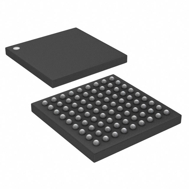
The Intel 10M08DFV81C7G is a Field Programmable Gate Array (FPGA) from the MAX 10 family, offering 8000 logic elements and 500 LABs/CLBs for flexible digital logic implementation. It includes 387072 bits of total RAM for on-chip data storage and 56 user I/O pins for interfacing with external components.
This device operates with a supply voltage range of 1.15V to 1.25V and is designed for surface mount assembly in an 81-UFBGA, WLCSP package (81-VBGA, WLCSP 4.5x4.4). The operating temperature range is 0°C to 85°C, suitable for commercial applications.
The FPGA is RoHS3 compliant and has an MSL level of 1 (unlimited). It is ideal for embedded systems requiring programmable logic with moderate logic density and I/O count.
The 10M08DFV81C7G has 8000 logic elements.
The supply voltage range is 1.15V to 1.25V.
It has 56 I/O pins.
The total RAM is 387072 bits.
It comes in an 81-UFBGA, WLCSP package (81-VBGA, WLCSP 4.5x4.4).
The operating temperature range is 0°C to 85°C.
It has 500 LABs/CLBs.