

| Distributor | Stock | Pricing | MOQ | PKG | Lead Time | Date Code | On Order Quantity | On Order Delivery | |
|---|---|---|---|---|---|---|---|---|---|
|
41 pcs
|
41 pcs | On Request | 1 | On Request | On Request | On Request | On Request | On Request |
| Category | |
| Manufacturer Name | |
| Mounting Type | |
| Number of I | |
| Number of LABs | |
| Number of Logic Elements | |
| Operating Temperature | |
| SVHC Present | |
| Supplier Device Package | |
| Total RAM Bits | |
| Voltage |
The Intel 10AX115R3F40E2SG is an Arria 10 family Field Programmable Gate Array (FPGA) designed for high-performance embedded applications. It features 1,150,000 logic elements and 427,200 logic array blocks (LABs), providing substantial programmable logic capacity. The device includes 68,857,856 bits of total embedded RAM for data buffering and storage.
This FPGA offers 342 user I/O pins for flexible interfacing with external components. It operates from a nominal supply voltage of 0.9V, with a minimum of 0.87V and maximum of 0.93V. The device is rated for a junction temperature range of 0°C to 100°C, making it suitable for commercial and industrial environments.
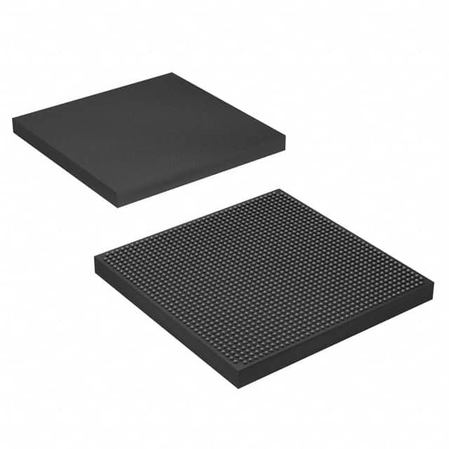
The 10AX115R3F40E2SG is supplied in a 1517-ball Fine-Pitch Ball Grid Array (FCBGA) package measuring 40x40mm, with surface mount mounting. The package has 1517 terminals positioned on the bottom, enabling high-density PCB integration.
The device has 1,150,000 logic elements.
It provides 342 I/O pins.
The supply voltage range is 0.87V to 0.93V, with a nominal of 0.9V.
It is packaged in a 1517-ball FCBGA (40x40mm) surface mount package.
The junction temperature range is 0°C to 100°C.
It has 68,857,856 bits of total RAM.
RoHS compliance is indicated as RoHS3 compliant, but this is unverified.