Onsemi’s upgraded silicon and silicon carbide F5BP Power Modules offer more power density and efficiency.

Solar storage facility.

Onsemi has released upgrades to its F5BP power integrated modules (PIM) that combine silicon and silicon carbide (SiC) technologies to deliver more power density and better efficiency in utility-scale solar inverter and battery energy storage system (BESS) applications.   

The improved PIMs increase the modules’ power rating from 300 kW to 350 kW. According to onsemi, the PIMs offer efficiency improvements equivalent to 2 MW per hour of power savings for a typical grid-scale solar generation facility, enough to power 700 homes.

Further, onsemi estimates that for each GW of installed capacity, a 0.1% improvement in efficiency equates to an operating savings of a quarter of a million dollars per year.

Enhancements drive the performance improvements to the integrated high-voltage IGBTs (insulated-gate bipolar transistors) and EliteSiC diodes that reduce switching losses and voltage flicker.

Sunrise for Solar

With an improving levelized cost of energy, solar power generation is quickly emerging as a preferred source for renewable power generation across the globe. To directly interface with the grid or power AC loads, sophisticated inverter circuits must convert the DC power generated from solar arrays to AC. Solar inverters must operate at utility-grade voltages and with high conversion efficiencies to remain competitive with other power sources.

Since solar energy production is intermittent, power generation plants also need local energy storage to balance the supply and demand for electricity and meet dispatchable power requirements for consumers. 

Large-scale battery energy storage systems are increasingly deployed to meet energy storage requirements in solar power facilities, and inverter circuits play a key role in connecting the BESS to the solar power source and the AC grid.  

Mixing Old and New Tech 

Onsemi’s F5BP-PIMs are an interesting mix of old and new technology, combining IGBT technologies in commercial use for decades with SiC devices recently used in broader commercial adoption in electric vehicle powertrains and similar high-voltage, high-power density applications. 

The upgraded power modules are available in either boost or inverter circuit configurations. The NXH500B100H7F5SHG module is configured as a two-channel flying capacitor boost module, with each channel using two 1000 V, 500 A IGBTs, and two 1200 V EliteSiC diodes. 

Each module is contained in a 112 mm x 62 mm x 12 mm enclosure with PCB mountable through hole pins. 

F5BP-PIM boost module schematic diagram.

F5BP-PIM boost module schematic diagram. Image used courtesy of onsemi

Within a solar inverter, the boost circuit elevates and regulates the operating voltage from the solar panels, which can vary with the solar energy’s intensity. For the inverter circuit to operate properly, the DC bus voltage must exceed the grid voltage peak.

Direct bonded copper substrates within the PIM reduce stray inductance and thermal resistance. A copper base plate reduces thermal resistance to the heat sinks by nearly 10%, allowing for higher power operation and improved reliability over time.

According to Sravan Vanaparthy, vice president of the Industrial Power Division, Power Solutions Group at onsemi, the new power modules will improve the efficiency of solar power generation, ensuring less energy is wasted and pushing forward the adoption of carbon-free, renewable energy sources.

P-DUKE Power XTBF500 Series of AC/DC Power Supplies | Digital Datasheet

AAC's Digital Datasheet video series provides insights into the specifications and applications of components, directly sourced from their datasheets, both for new and familiar products.

P-DUKE Power XTBF500 Series of AC/DC Power Supplies

P-DUKE XTBF500 series is a rugged 500W AC/DC power supply solution, combining the TBF500 with essential peripherals to deliver durable and flexible power options. With a universal input range of 85 to 264 VAC, the XTBF500 series provides multiple output voltages adjustable by ±10% and achieves up to 93% conversion efficiency. It features advanced capabilities like a Power Good signal, current share function, and comprehensive protection modes to ensure reliable performance in diverse environments. The series is designed for optimal thermal management, allowing operation at full load up to 40°C through conduction cooling or forced air cooling, and is rated for altitudes up to 5000 meters. Compliant with IEC/UL/EN 62368-1 and EMC standards, it is ideal for applications in 5G communication systems, industrial printers, energy storage systems, defense equipment, and factory automation. The XTBF500 series offers high efficiency, robust protection, and easy integration, making it a dependable choice for challenging industrial environments.

EVLO Expands Portfolio with Launch of EVLO SYNERGY – A High-Density 5 MWh Battery Storage Solution

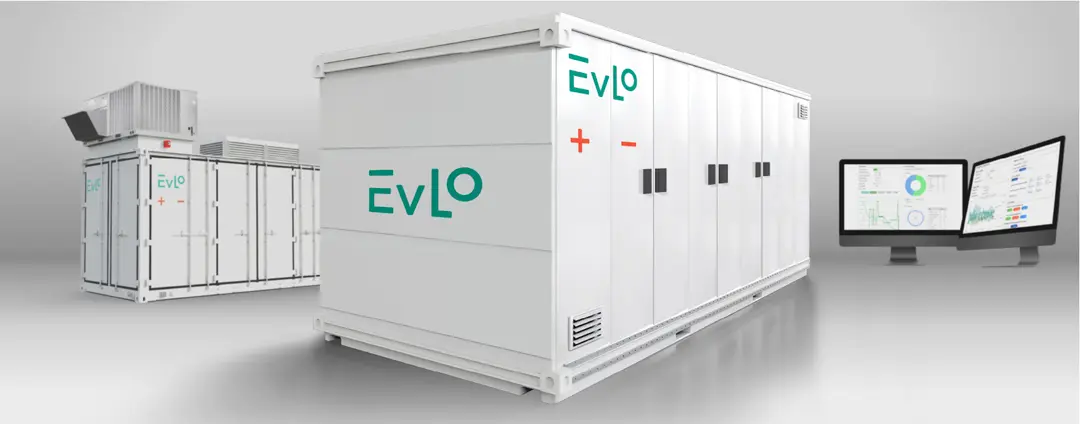
EVLO Energy Storage Inc. (EVLO), a fully integrated battery energy storage system (BESS) provider and wholly owned subsidiary of Hydro-Québec, announces EVLO SYNERGY, a new 5-megawatt-hour (MWh) BESS in a 20-foot enclosure. EVLO SYNERGY is the latest addition to EVLO’s portfolio of BESS products dedicated to the integration of renewable energy, participation to capacity services, and the resiliency of the electrical grid.

Engineered to serve the evolving needs of today’s market, EVLO SYNERGY’s high energy density unlocks a highly competitive cost of ownership for large-scale projects at the heart of modern energy infrastructure. Its efficient design reduces land use, construction materials, and project timelines, making it the optimal solution for large-scale projects.

“This launch is a significant expansion of our portfolio, emphasizing our commitment to advanced, safe, and cost-effective energy solutions that support our customers’ requirements for clean energy projects,” says Sonia St-Arnaud, president and CEO of EVLO. “As with all of our solutions, EVLO SYNERGY is supported by EVLO’s best-in-class customer experience, which ensures a collaborative partnership throughout a project’s entire lifecycle."

System specifications:

    Nominal energy capacity of 5 MWh and a versatile duration of 2-4 hours.
    Fully tested and integrated, minimizing onsite work.
    End-to-end fire safety: Meets NFPA 69 standard and is UL 9540 certified.
    Running for up to 9,125 cycles over 25 years without the need for battery replacements.

EVLO SYNERGY combines the latest high-density lithium-iron-phosphate (LFP) technology and EVLO's top-tier integration capabilities. It comes with industry-leading operation and maintenance service to ensure peak system performance and optimize return on investment across the entire project lifecycle.

EVLO SYNERGY is leveraged by EVLOGIX Site Controller and Asset Manager, EVLO’s NERC CIP-ready energy management system (EMS). EVLO’s portfolio also includes EVLOFLEX, a utility-scale BESS.

Energy storage provides frequency regulation, peak shaving, capacity services, renewable energy integration, and a range of other cost-effective grid stabilizing services. Globally, energy storage capacity is projected to exceed 1 terawatt-hour by 2030. This rapid growth, coupled with the increasing size of individual projects, will necessitate that energy storage adoption be as efficient and cost-effective as possible. Next-generation, high-density solutions like EVLO SYNERGY are critical in helping utilities provide reliable, affordable, and sustainable electricity while ensuring long-term grid security and resilience.

EVLO will unveil EVLO SYNERGY at the renewable industry conference RE+ in Anaheim, California. Visit Booth #N89019 on September 10, 2024, at 4 p.m. for an exclusive presentation.

About EVLO Energy Storage Inc.

EVLO Energy Storage Inc. (EVLO) is a fully integrated battery energy storage systems and solutions provider and subsidiary of Hydro-Québec. EVLO’s utility-scale battery energy storage systems and controls software deliver superior safety and reliability backed by decades of R&D. Its comprehensive services are led by a veteran team of industry experts passionate about partnering with customers to build a cleaner, more resilient energy future.

Onsemi Unveils Next-Gen SiC MOSFETs

EliteSiC M3e MOSFET.

Global energy demands are projected to soar over the next decade, making the need for increased power density in semiconductors paramount. Onsemi has released its latest generation of EliteSiC M3e MOSFETs, which are designed to reduce carbon emissions and increase the use of renewable sources in the global energy transition. 

“What onsemi brings to the table is to really enable this movement toward more electrification and the movement toward using renewable energy instead of the fossil fuels, leading to a more sustainable healthier planet that we can leave for our posterity,” Mrinal Das, Senior Director of Technical Marketing for the Advanced Power Division with onsemi, told EEPower in a press briefing.

Understanding Silicon Carbide

Diamond is completely carbon. Silicon carbide is much like diamond, except it is 50% carbon. It’s a diamond with some silicon, alternating layers of silicon and carbon. 

While diamond has phenomenal electrical properties like high dielectric breakdown strength for low resistance and high thermal conductivity for more current flow, so does SiC. However, silicon carbide can be manufactured similarly to silicon, allowing higher voltages and efficiencies. 

“This is the powerful impact of silicon carbide. You get the benefit of a next-generation semiconductor while still having the manufacturability of today's incumbent,” Das said. “So, very rare combination, which is why silicon carbide is the leading next-generation semiconductor to replace silicon. The combination of these two material properties really delivers a lot of value at the system level, which is why the silicon carbide is such a prominent player as a next-gen semiconductor.”

Onsemi’s 3rd Generation SiC MOSFETs

The EliteSiC M3e MOSFETs, or M3e as they are called, join M3S and M3T as a 1200 V, 11 mΩ SiC MOSFET, which is a bare dye for traction inverters in electric vehicles.

Compared to previous generations, conduction losses are reduced by 30%, enabling a traction converter with 20% more power and improving power density, while switching losses can be lowered by up to 50%—all in a planar MOSFET. 

“These are not trench MOSFETs. The advantage of staying on planar is that you can still connect to the legacy of work that has been done on that planar topology so that there's been 40 years of work done in R&D and 15 years of field-proven demonstration of quality and reliability,” Das said. “And it is truly the technology of today.”

Onsemi MOSFETs

Image used courtesy of onsemi

M3E is rated for short-circuit withstand capability, meaning that the motor can survive short-circuit events in applications with a motor and load. 

The M3e MOSFETs also offer the industry’s lowest specific on-resistance (RSP) with short circuit capability, according to onsemi, critical for traction inverters. Packaged in onsemi’s state-of-the-art discrete and power modules, the 1200 V M3e die delivers substantially more phase current than previous EliteSiC technology, resulting in 20% more output power in the same traction inverter housing. Conversely, a fixed power level can now be designed with 20% less SiC content, saving costs while enabling the design of smaller, lighter, and more reliable systems.

A Look at the Future

The EliteSiC M3e MOSFETs are fundamental to enabling the performance and reliability of next-generation electrical systems at a lower cost per kW and will influence the adoption and effectiveness of electrification initiatives. Operating at higher switching frequencies and voltages while minimizing power conversion losses makes this platform essential for various automotive and industrial applications, such as electric vehicle powertrains, DC fast chargers, solar inverters, and energy storage solutions.

EliteSiC M3e wafer

EliteSiC M3e wafer. Image used courtesy of onsemi

Onsemi is leading innovation across its silicon carbide roadmap—from die architectures to novel packaging techniques—that will continue to address the industry demand for increased power density.

With each generation of silicon carbide, cell structures will be optimized to push more current through a smaller area efficiently, increasing power density. Coupled with onsemi’s advanced packaging techniques, performance is maximized, and package size is reduced. By applying the concepts of Moore’s Law to silicon carbide development, onsemi intends to develop multiple generations in parallel and accelerate its roadmap to bring several EliteSiC products to market through 2030.   

Toshiba Demos New Switching Topology for Non-Isolated DC-DC Converters

Non-isolated buck DC-DC converter power supplies

The new topology eliminates the need for a transformer and significantly reduces the number of capacitors in DC-DC converter ICs. Toshiba recently announced a new non-isolated DC-DC converter technology that operates from 48 V to 1 V. These devices address conduction losses associated with mounting server and data center demands, which increases load currents in DC-DC converters. The result of these higher load currents and conduction losses is heat and lower overall efficiency.

To mitigate these losses, industry standards have raised the input voltage from 12 V to 48 V. This reduces the current for a given power level, thus lowering conduction losses. However, this shift also introduces new challenges for DC-DC converter designs, particularly with the buck topology.

Toshiba claims its new star-delta switching topology reaches the industry’s highest current densities while negating the need for a transformer for DC-DC converter ICs with 48-V input and 1-V output.

Toshiba Leverages Star-Delta Switching Topology

At the 2024 IEEE Symposium on VLSI Technology & Circuits, Toshiba demonstrated its new 48 V to 1 V non-isolated DC-DC converter technology. The test device achieved current densities of up to 790 mA/mm² and a high power conversion efficiency of up to 88%.

The proposed star-delta switching network

The proposed star-delta switching network. Image used courtesy of Toshiba

According to Toshiba, its star-delta switching topology eliminates the need for transformers, which are typically used in isolated topologies to manage pulse-width expansion. Instead, Toshiba uses a hybrid configuration of inductors and capacitors, judiciously controlled by FETs, to significantly reduce the volume and number of external components. Toshiba claims that its star-delta topology reduces the capacitor count per pulse-width expansion ratio from 0.5 to 0.6, as opposed to 0.8 to 1.0 in traditional non-isolated hybrid topologies. 

Toshiba demonstrated the effectiveness of this topology with a suite of test chips. The company developed a bootstrap circuit that cut layout area by up to 61% and a level shifter circuit that supports an active bias current scheme, reducing bias current by up to 92%. 

Eliminating the Bulk of Transformers and Capacitors

In a buck converter, the pulse width driving the power switch must be four times shorter than 12 V to increase the input voltage to 48 V. This reduced pulse width increases switching losses as the transitions between on and off states become more frequent and less efficient. These switching losses then directly degrade the overall power conversion efficiency of the system.

Designers often use transformers in isolated topologies to address these efficiency issues. While transformers expand pulse width and prevent switching losses, they also add significant bulk to a design, which is problematic in applications where space is constrained.

Non-isolated multiport converter

Non-isolated multiport converter. Image used courtesy of MDPI

Non-isolated hybrid topologies are a compact alternative. These designs use a combination of inductors and capacitors to manage pulse width expansion without bulky transformers. Compared to transformer-based solutions, this approach can reduce the overall volume of the converter by a factor of 10 to 100. Despite these space-saving advantages, hybrid topologies introduce their own challenges.

One significant drawback is the requirement for a large number of capacitors—typically 0.8 to 1.0 capacitors per pulse-width expansion ratio. This increased capacitor count leads to higher external component density and congestion in pin wiring, complicating the PCB layout and increasing mounting costs. The additional capacitors and complex wiring elevate manufacturing costs and pose challenges to system reliability and maintenance.

The Star-Delta Solution

Toshiba says its star-delta switching topology merges switching layers on the input side where the current is comparably small. Because each switching layer requires at least one capacitor, reducing the number of switching layers also cuts the total number of capacitors.

AGV Wireless Charger

EnerSys now offers the NexSys Air wireless charger designed for automated guided vehicles (AGVs). The charger features contact-free charging pads, reducing wear and maintenance related to physical connections. Compatible with various battery types, including flooded lead acid, thin plate pure lead, and lithium-ion, it accommodates diverse AGVs, charging schedules, and facility setups. Featuring a small footprint, the chargers offer layout flexibility and are equipped with user-friendly touchscreen controls and safety features like foreign object detection and live object detection to ensure worker and equipment safety.

Microchip Releases Chipset Solution for Designing Onboard EV Chargers

Microchip combined EV on-board charging components

The new design on-board charger (OBC) chipset and accompanying white paper provide a trusted path forward for battery EV and plug-in hybrid vehicle designers.

Microchip has announced a new onboard charger (OBC) solution that combines the company's intelligence, power factor correction, signal generation, and high-voltage, and high-current drive components. These include Microchip's dsPIC33C digital signal controller (DSC), the MCP14C1 isolated SiC gate driver, and SiC MOSFETs. The solution promises to speed up time to market for EV developers for both battery-powered EVs and plug-in hybrid EVs.


Microchip combined EV onboard charging components. 

Microchip has also released a white paper alongside the OBC outlining how it can improve charge movement into a battery pack and back out again.

Control

For many years, designers have used the Microchip dsPIC in motor control power inverters and charging circuits. In addition to providing the basics, like high-resolution pulse width modulation (PWM) and analog-to-digital converters (ADC), the dsPIC offers advanced digital signal processing functions to help with the feedback and analysis aspects of power electronics.

The dsPIC33C DSC microcontroller family is AEC-Q100 qualified for use in automotive applications. The microcontrollers feature a dual-core architecture. One core can be dedicated to control and automotive communications, while the other handles signal processing and complex tasks like power factor corrections and modulation. Separating these tasks increases both performance and reliability.

The dsPIC's signal processing capabilities enhance control algorithms, voltage regulation, and current limiting. The DSP's efficient algorithms deliver highly controlled charging under a wider variety of scenarios.

Drive

The MCP14C1 isolated gate driver is also AEC-Q100 qualified. It comes in multiple chip packaging: the SOIC-8 wide body for reinforced isolation and the SOIC-8 narrow for standard isolation. The driver's source and sink 5 A of current are designed for driving silicon carbide (SiC) MOSFETs. The driver chips support undervoltage lockout, an important requirement when driving SiC MOSFETs.

The driver chips are offered with a split output, allowing designers to use external gate resistors for pull-up or pull-down adjustments. The split output and compatibility with resistor pulls eliminate the need for external diodes, reducing cost and improving reliability. Isolation is also a critical component of power electronics in the KW regime. The MCP14C1 uses internal capacitive isolation, which reduces noise and inhibits unintended triggering.

Power

Rounding out the set are AEC-Q100-qualified SiC power MOSFETs in D2PAK-7 XL surface-mount packages. Microchip offers a wide selection of SiC MOSFETs that fit into automotive-qualified onboard charging solutions. Due to the higher bandgap and better thermal breakdown characteristics of SiC, SiC MOSFETs deliver higher voltages and current capacities.

dsPIC MCU, MCP14C1 gate drivers, and SiC MOSFETs

dsPIC MCU, MCP14C1 gate drivers, and SiC MOSFETs. 

The D2PAK-7L XL package complements the device's SiC-related advantages by providing five parallel source sense leads. These leads increase current capacity and reduce switching losses.

DSP MCUs, Gate Drivers, and SiC MOSFETs

In a typical EV charging scenario, power is presented to the vehicle at one of many different AC or DC voltages and delivered at one of several current flows. EV onboard charging systems take that power from the cable and convert it into a form that can be accepted by the EV’s battery pack. Such a circuit requires intelligence and power drive capacity tuned to the specific design attributes of the battery pack.

DC-DC converter block diagram for an onboard charger.

DC-DC converter block diagram for an onboard charger. 

Proper charging circuit design can have a major impact on automotive range, battery life, and EV customer satisfaction. Yet designing from scratch is an incredibly complex and difficult process. By equipping the design with in-house components, users of the Microchip solution can have greater assurance that their designs will work reliably in the field. The Microchip solution uses proven components that are compatible with each other.

Broad Functionality From One Solution

Microchip’s reference designs include complete charging solutions that can be easily adapted to fit a wide variety of onboard charging scenarios. In addition to demonstration applications, reference designs, and built-up reference boards, the solution includes development and simulation tools, multiple component options, and a dedicated support team.

All images used courtesy of Microchip.

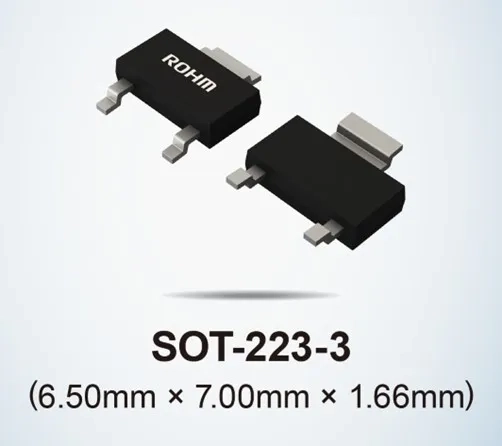
Rohm offers a new five-model portfolio of 600-V SJ MOSFETs, housed in a smaller SOT 223-3 package, saving space in power supplies, pumps and motors.

Rohm Semiconductor has added a new five-model lineup of compact 600-V Super Junction (SJ) MOSFETs, targeting small lighting power supplies, pumps and motors. The new offering of SJ MOSFETs include the R6004END4, R6003KND4, R6006KND4, R6002JND4 and R6003JND4.

Rohm explained that it has been difficult to reduce the size of the SJ MOSFETS, while maintaining an optimized balance between high breakdown voltage and low on-resistance. In response, the company developed the new models in the SOT-223-3 package (6.50 × 7.00 × 1.66 mm), which offers a smaller and lower profile form factor without sacrificing the performance of conventional products.

Compared to the conventional TO-252 package (6.60 × 10.00 × 2.30 mm), the new power MOSFETs reduce area and thickness by 31% and 27%. Rohm also noted that the same land pattern (footprint) as the TO-252 package can be used, enabling mounting on existing circuit boards without modification.

Three of the models are optimized for compact power supplies. The R6004END4 offers low noise while the R6003KND4 and R6006KND4, capable of high-speed switching, are suited for low loss and high efficiency applications. These devices target applications such as lighting, air conditioners and refrigerators.

The R6002JND4 and R6003JND4 devices use Rohm’s proprietary PrestoMOS power MOSFET technology to achieve significantly lower switching losses by speeding up reverse recovery time (trr) of the built-in diode, making them well-suited for motor-equipped devices such as pumps, fans and copiers.

The SJ MOSFETS are available through Rohm’s online distributors, including Digi-Key, Mouser and Farnell. Rohm expects to expand the family with different packages and lower on-resistance ratings.

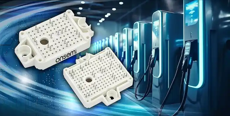
Onsemi adds nine new EliteSiC power integrated modules for DC ultra-fast EV chargers and energy storage systems.

Onsemi has expanded its EliteSiC power integrated modules (PIMs) with nine new devices for enabling bidirectional charging capabilities in DC ultra-fast electric vehicle (EV) chargers and energy storage systems (ESS). The EliteSiC devices are based on the company’s Gen3 M3S SiC MOSFET technology, which claims the industry’s lowest switching losses and highest efficiency.

The PIMs feature scalable output power from 25 kW to 100 kW, which enables multiple DC fast charging and energy storage systems platforms including bidirectional charging. They are available in industry-standard F1 and F2 packages with the option of a pre-applied thermal interface material (TIM) and press-fit pins.

The silicon carbide-based devices are reported to improve system cost with higher efficiency and simpler cooling mechanisms that can reduce size by up to 40% and weight by up to 52% compared to traditional silicon-based IGBT solutions. The result is smaller and lighter charging platforms to develop a “scalable network of DC fast chargers that can charge electric vehicle batteries up to 80% in as little as 15 minutes,” onsemi said.

This is significant because nearly half of U.S. consumers said the reason for not purchasing an EV is the access to charging and the ability to charge quickly, according to J.D. Power’s 2023 Electric Vehicle Consideration Study.

 The increased demand for electricity “will also put a tremendous strain on current electrical grids, potentially overloading them,” onsemi said. However, bidirectional charging is emerging as a solution to implement vehicle-to-grid, which allows for regular battery charging and the ability to use an EV as an energy storage system to power homes when needed, the company said.

 The PIM devices support key topologies such as multi-level T-type neutral point clamp (TNPC), half-bridge and full-bridge, which gives designers the flexibility to pick the right PIM for power conversion stages in their DC fast charging or ESS applications. In addition, onsemi offers advanced piecewise linear electrical circuit simulation (PLECS) models through its Self-Service PLECS model Generator and application simulation with the Elite Power Simulator, introduced earlier this year. Check out the white paper to learn more about the power converter technologies for DC fast and ultra-fast charging.

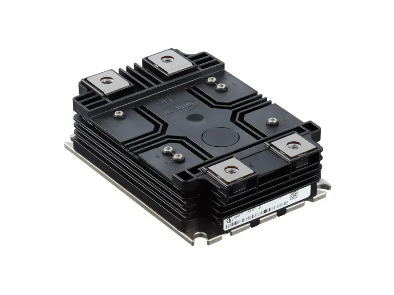
Infineon’s XHP 3 IGBT modules simplify paralleling and enable the downsizing of drives without sacrificing efficiency.

To meet growing demand for further downsizing and integration, Infineon Technologies AG has launched the 4.5-kV XHP 3 IGBT modules, targeting large conveyor belts, pumps, high-speed trains, locomotives, as well as commercial, construction and agricultural vehicles (CAV). The XHP family is comprised of a 450-A dual IGBT module with TRENCHSTOP IGBT4 and an emitter-controlled diode, and a 450-A double diode module with an emitter-controlled E4 diode.

The company said the new IGBT modules “will fundamentally change the landscape for medium voltage drives (MVD) and transportation applications operating at 2,000 to 3,300 V AC in 2- and 3-level topologies.”

Both modules offer improved isolation of 10.4 kV and help simplify paralleling and downsizing without sacrificing efficiency, Infineon said. “Previously, complex busbars were required to parallelize switching modules, resulting in complicated design efforts and leakage inductance.”

The new XHP family design simplifies paralleling by placing the connections side by side, resulting in the need for only a single straight busbar for paralleling.

The 4.5-kV XHP modules also reduce the number of units needed for a design. Application requirements can be reduced to two dual switches and a smaller double diode from designs that traditionally require multiple single switches and a double diode.

The combination of the XHP 3 FF450R45T3E4_B5 dual switch and the DD450S45T3E4_B5 double diode also deliver a smaller footprint and lower cost. Infineon’s previous IGBT solutions required four 140 × 190 mm² or 140 × 130 mm² switches and one 140 × 130 mm² double diode. With the new XHP family, the solution can be reduced to two 140 × 100 mm² dual switches and a 140 × 100 mm² double diode. Both modules are available now.