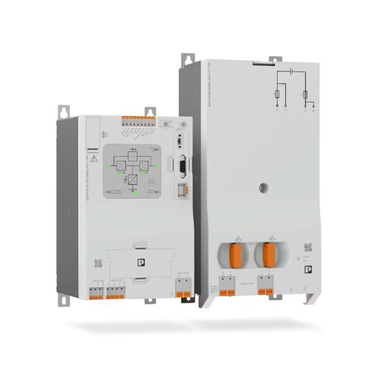
The Quint HP AC uninterruptible power supply (UPS) includes Phoenix Contact’s UPS IQ technology and battery management system. The modular Quint HP AC UPS features a panel-mounted platform with a battery capacity range of 7-200 amp hours and can monitor up to five battery units. The new UPS’s batteries are hot-swappable. The integrated fuses and fan are also easy to replace. The Quint HP UPS has a removable communications card for USB and RS-232/RS-485 for communication to PCs, RTUs and HMIs. If a power failure occurs, the Quint HP AC UPS ensures an uninterrupted transition to buffer mode and back again. Mains input and output voltages are synchronous.
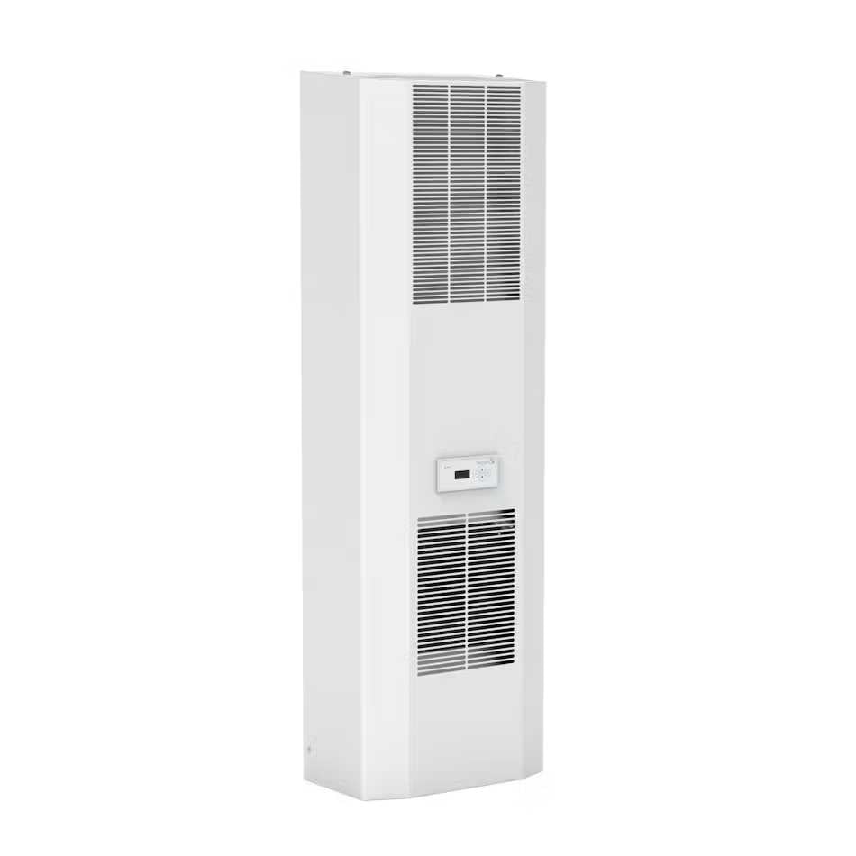
The new X-Series of Pfannenberg cooling units feature an optimized control algorithm using inverter technology which allows for the precise adjustment of cooling power required to maintain the temperature within the enclosure. The X-Series guarantees temperature control within a tolerance of +/- 0.1K. The X-Series includes two models: the 6X1E, covering a power range from 1000W to 2800W, and the 6X2E, ranging from 2000W to 4500W. Both units are equipped with an RS 485 interface and Modbus RTU protocol. Units will be available in the standard side or surface mount as well as the recessed mount. The units are also UL certified.
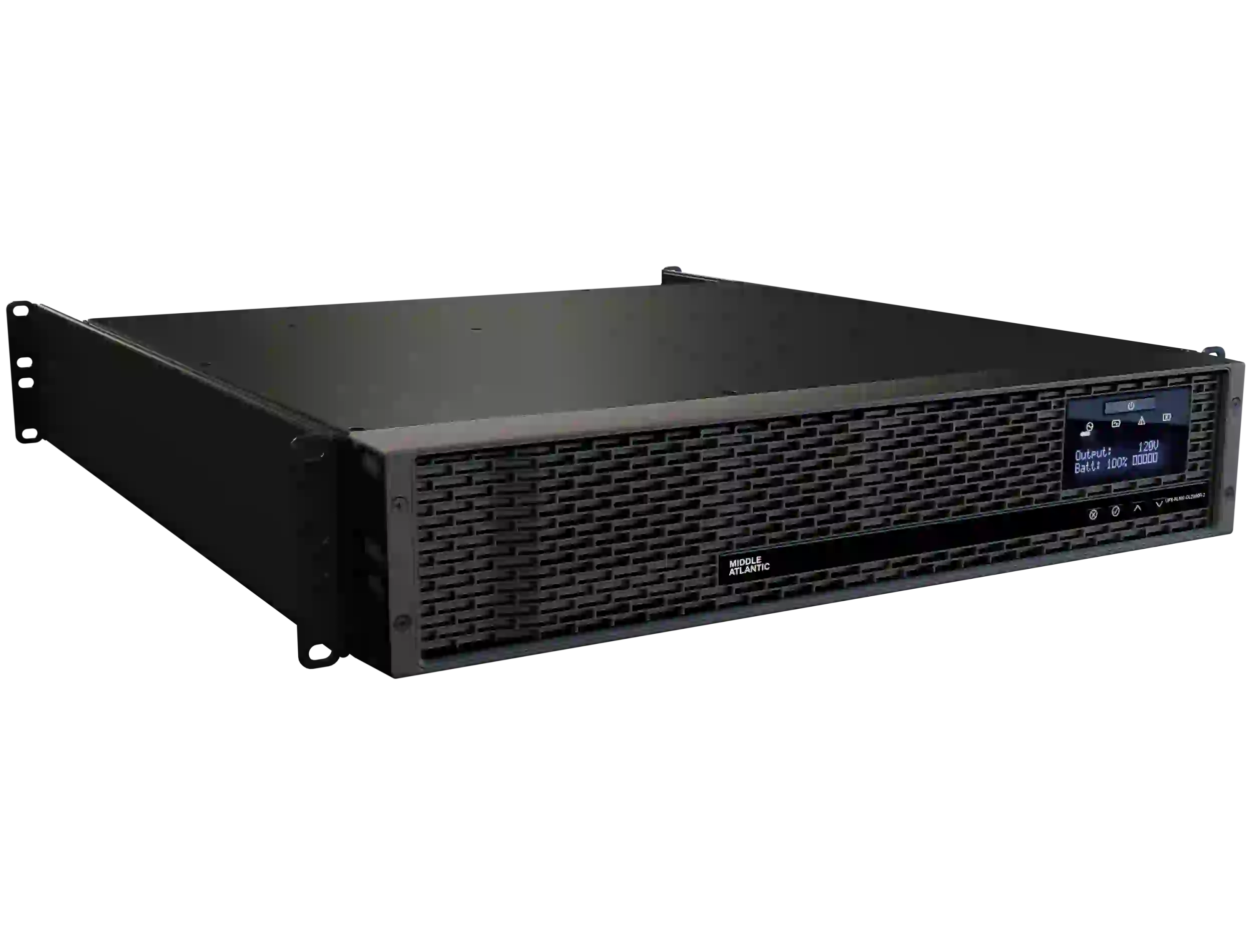
Middle Atlantic Products, a brand of Legrand | AV, recently announced the latest additions to its NEXSYS™ AV power distribution and backup platform, the NEXSYS Online UPS Series. The NEXSYS Online UPS carries forward the reliability, protection, and control that the platform introduced to the market, now in new options to fit today’s most demanding and sensitive AV systems. Available in 12 configurations, the NEXSYS Online UPS Series offers six or eight outlets with bank or individual outlet control, in 15 Amp 1000VA and 1500VA, 20 Amp 2000VA, and 30 Amp 3000VA models.
“NEXSYS provides the industry with power products designed, engineered, and built for AV, a Middle Atlantic promise on our power products for over two decades,” said Nyron Kahrim, Product Manager for Middle Atlantic UPS Power Products at Legrand | AV. “The new NEXSYS Online UPS family stands firm in that commitment. It’s built with premium components to keep AV systems running smoothly and reliably, even during power outages or anomalies.”
The Middle Atlantic NEXSYS Online UPS Series ensures a strong foundation for any AV system. The Energy Star-certified and U.S. Department of Energy-compliant solutions deliver pure sine wave output with an online, double-conversion topology with zero transfer time, providing the cleanest and most reliable power to connected equipment, especially the most sensitive. The series includes eight outlet models in either bank control with two four-outlet banks or individual control for all eight outlets, making it the first online UPS with individual outlet control in the AV market. The 3000VA models feature six outlets with individual outlet control or bank control. For bank control, the outlets are arranged into two banks with three outlets each that include six NEMA 5-20R outlets. The 3000VA models also include an additional NEMA L5-30R outlet that is not controlled but always on when the UPS is turned on.
Every unit comes assembled and connected right from the factory, saving integrators time during installation. With preinstalled rack ears with “4-Post” mounting brackets and a connected battery, installers can quickly mount and plug it in. Setting and notifications, such as battery replacement, can be customized via NEXSYS Power Management Software. In addition, the NEXSYS UPSs are RackLink™ compatible for remote monitoring and management including RackLink Cloud. Installers can easily access and service the hot-swappable battery from the front access panel without disrupting the system.
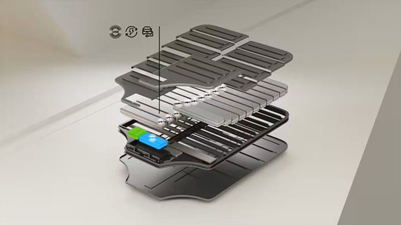
NXP is taking a new approach to EV battery management to extend range and decrease assembly costs.At this year’s Electronica, NXP Semiconductors announced the "industry's first ultra-wideband (UWB) wireless battery management system (BMS)". Traditional BMS architectures, reliant on intricate wiring and labor-intensive assembly, can constrain performance and cost.
With EV adoption accelerating, manufacturers are looking for novel solutions to streamline production, extend vehicle range, and support a broader platform portfolio—all of which UWB promises to deliver.
NXP Optimizes BMS Power With UWB Solution
Integrated into a FlexCom chipset, NXP's new UWB solution supports both wired and wireless configurations using a unified software architecture and safety libraries. This approach allows automotive manufacturers to reuse software across different platforms, accelerating development cycles and reducing engineering complexity.
The UWB solution operates over a broad spectrum between 6.0 GHz and 8.5 GHz to deliver data transmission that NXP claims surpasses the limitations of traditional narrow-band technologies. NXP says the UWB BMS provides reliable communication by addressing challenges like reflections and frequency-selective fading, both of which are common in metal-enclosed battery packs.
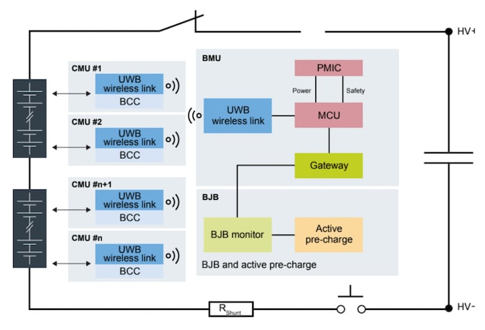
Block diagram of a battery pack with wireless inter-module communication.
Thanks to these advances, NXP claims that the UWB BMS achieves performance benchmarks with a packet error rate below 10-6, a fourfold increase in bandwidth (7.8 Mbps), and twenty times faster synchronization than conventional systems. Additionally, the solutions reportedly feature a 5x faster packet rate and 40% power savings than conventional options. These capabilities help optimize the BMS' power consumption and enhance EV range and vehicle uptime.
Why Ultra-Wideband for Battery Management?
In BMS, UWB technology replaces traditional wired connections with high-bandwidth wireless communication.
UWB operates across a wide spectrum, typically between 6.0 GHz and 8.5 GHz, using short pulses for data transmission. This technique yields robust signal propagation within electrically noisy and reflective environments, such as metal-enclosed battery packs. Unlike narrow-band systems that are prone to fading and interference and rely on sinusoidal carrier frequencies, UWB leverages reflections to enhance signal strength and maintain reliable communication.

Application diagram of NXP’s UWB BMS.
In a UWB-enabled BMS, data from individual battery cells—such as voltage, temperature, and state of charge—is transmitted wirelessly to the battery management unit (BMU). This eliminates the need for physical wiring harnesses, connectors, and intricate manual assembly processes. Removing these components increases energy density and enables more compact and efficient battery designs, extending electric vehicles (EVs) ranges.
UWB offers other advantages over conventional BMS solutions, too. It simplifies mechanical and electrical integration, which accelerates design cycles and reduces engineering complexity. The wireless architecture decreases labor costs, enhances safety in high-voltage environments, and improves serviceability during maintenance. Additionally, the technology supports scalable and reusable designs, allowing manufacturers to adapt a single architecture across multiple platforms.
Back to the EV Basics
NXP's UWB-enabled BMS reflects a growing emphasis on improving the technological foundation for electric vehicles. By addressing long-standing challenges associated with wired BMS, UWB may extend range and reduce the manufacturing constraints of EVs. NXP's UWB BMS solution is currently available to OEMs for evaluation, and development options will be ready in Q2 of 2025.
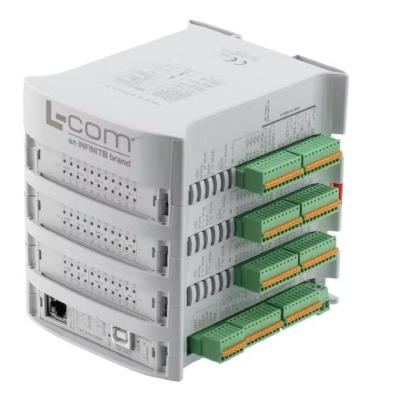
A new line of open-source Arduino PLCs can be programmed using free open-source Arduino software. These PLCs feature options of 19, 21, 38, 42 or 58 analog and digital inputs and outputs (I/O). They accept I/O or sensors and power as inputs and deliver outputs to actuators and human machine interfaces. The PLCs feature network connection via Ethernet, multi-point RS-485 and point-to-point RS-232. Three new L-com power supplies convert power from AC to DC to run PLCs and other devices. The L-com options consist of a 30-watt power supply with a 12V DC output, 120 watts with 24V DC, or 220 watts with 24V DC. They have universal power inputs of 100 to 240V AC for the 30-watt and 120-watt models, and 200 to 240V AC for the 240-watt model. The power supplies have overvoltage and overcurrent protection and an LED indicator.

HiKOKI Power Tools has launched the BSL3640MVT Multi Volt Battery, its latest battery innovation. The new 8.0Ah battery, which charges in just 40 minutes, uses Tabless cell technology, which means increased power, faster charging times and longer runtimes to meet the needs of professionals tackling both light and heavy-duty applications.
Designed to power both 36V and 18V HiKOKI power tools, the BSL3640MVT delivers up to 2,160W of power – 50% more than its predecessors – so it is ideal for demanding tasks like sawing, drilling, cutting and grinding, regardless of whether its heavy-duty construction projects or smaller, more intricate jobs.
The 8.0Ah Multi Volt BSL3640MVT uses tabless cell technology which significantly reduces internal resistance and heat. Traditional batteries use two tabs as current paths which can create a bottleneck. Instead of two current paths, the battery has countless current paths. This improves power output and allows for longer runtimes, even under extreme conditions. It also reduces the build-up of heat so the battery remains cool during use and experiences less wear and tear.
The quick charging time is another key benefit. When paired with the UC36YSL2 charger, the battery fully charges in just 40 minutes, minimising downtime on job sites. This means less waiting and more productivity for those who rely on their tools to get the job done efficiently.
The BSL3640MVT is built to withstand tough job site conditions. It has an impact-resistant design and a rubber over-moulded base so even if dropped or accidentally bashed, this battery will continue to do its job.
HiKOKI’s new BSL3640MVT Multi Volt Battery is a great battery upgrade for anyone who wants quick charging, extended runtimes and long life from their power tools. Whether you’re tackling heavy-duty applications or quick fixes, this battery ensures you’ll have the power and runtime you need to get the job done right.
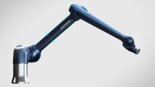
The P-Series cobot lineup features lower power consumption when compared to similar payload cobots via its built-in gravity compensation mechanism, inherent wrist-singularity free and a 5 degrees-of-freedom movement with the 4th axis removed and 6th axis speed increased to 360 degrees/second. All P-Series cobots hold the highest PL (e) and Cat 4 safety ratings to ensure a full-powered, maximum-safety experience. The first cobot available in this lineup is the P3020, which offers a payload of 30kg and reach of 2,030mm, bringing the ability to palletize from floor to 2m high using its fixed base without a lift.
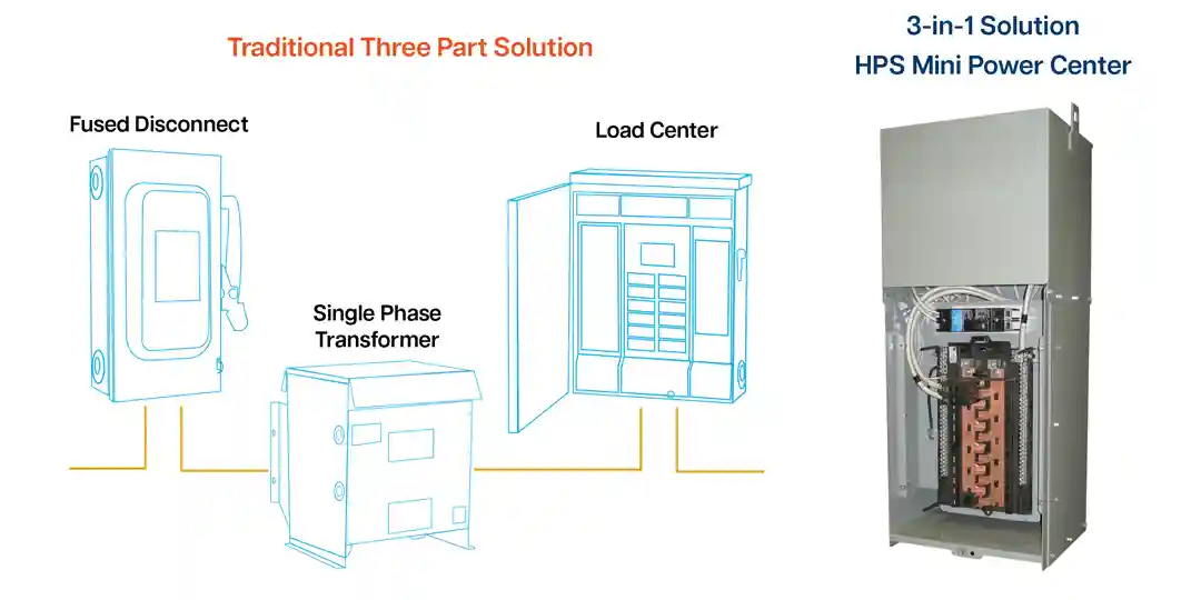
Hammond Power Solutions (HPS), a leader in dry-type transformers and power quality solutions, is pleased to announce the expansion of our Mini Power Center, now featuring both 480V and 600V primary solutions. This expansion underscores our commitment to serving our customers needs and delivering versatile and efficient solutions.
Modern electrical distribution systems need to be efficient in both space and cost. HPS mini power center addresses these needs with less space, and reduced installation time by up to 25% compared with a traditional three-part solution.
This convenient pre-wired solution combines a primary and secondary main breaker, secondary power panel and a dry-type shielded transformer in a Type 3R enclosure.
Key Benefits:
Saves Time: Prewired, ready-to-use design simplifies installation time by up to 25%*.
Space Savings: Compact design saves up to 50% less space*.
Reliable Protection: Built in circuit breakers provide reliable protection for rugged industrial environments.

ST designed its newest STPower silicon carbide (SiC) MOSFETs to improve efficiency, power density, and robustness for EV powertrains and charging circuits.STMicroelectronics has released the fourth generation of its STPower silicon carbide (SiC) MOSFET technology. ST claims the new MOSFETs will offer higher performance levels in terms of efficiency, power density, and robustness.
While suited to a range of high-voltage and high-power density industrial and e-mobility applications, the new generation MOSFETs specially target EV traction inverters, the essential element of an EV powertrain that converts DC power from the battery pack to three-phase AC to power the motor.
The new SiC MOSFETs will be available with 750-V and 1,200-V ratings to support both 400-V and 800-V battery bus voltages, the latter providing faster vehicle charge times and longer ranges. 750-V variants of the new MOSFETs have completed qualification, and the 1,200-V models are set to complete qualification in the first quarter of 2025. Commercial availability will follow soon after. In addition to EVs, the new MOSFETs can serve high-power industrial applications such as solar inverters, energy storage solutions, and data centers.
Improving EV Performance
Within an EV’s powertrain, the traction inverter converts DC power from the battery to three-phase AC to drive the EV’s electric motor. To do this, the traction inverter uses a bridge circuit constructed from discrete power MOSFETs or carefully sequenced power modules to generate the required AC motor drive waveforms. The performance of the inverter and its switching power components greatly impact the overall performance of the EV.

EV powertrain block diagram. Image used courtesy of STMicroelectronic
ST’s new Gen 4 SiC MOSFETs feature a lower on-resistance (RDS(on)) than prior generation devices; when the switches are on, they generate fewer I2R losses. This translates to more efficient power conversion and a lighter, more compact solution because of fewer thermal management concerns—all critical factors to an EV’s range, charge times, and cost.
Considering a figure of merit (FOM) of die size x RDS(on), ST claims that its Gen 4 SiC MOSFETs require 12% to 15% less silicon area to achieve a similar on-resistance to a Gen 3 device, saving space and reducing per-unit costs. Along with a lower RDS(on), higher switching speeds and increased robustness also contribute to a smaller, lighter, and less expensive EV drivetrain.
ST's SiC Technology Roadmap
ST plans to continue delivering new SiC solutions through 2027 and beyond. To do this, the company has invested in a vertically integrated silicon carbide supply chain from substrate manufacturing to final device assembly and packaging. For the coming fifth generation of its SiC technology, ST is exploring new planar structures to improve power densities and lower on-resistances.
![]()
Silicon carbide wafer. Image used courtesy of STMicroelectronics
According to the company, ST has supplied more than five million STPower SiC devices globally for EV applications, including for traction inverters, onboard chargers (OBC), DC-DC converters, and charging stations.

The new chip measures currents, voltages, and temperatures in EV and hybrid-EV battery packs.NXP Semiconductor has released the MC33777 battery junction box controller chip designed to monitor and protect battery systems in EV and hybrid-EV (HEV) vehicles.
Compliant with ASIL-D requirements, the new IC redundantly measures battery pack currents, voltages, and temperatures. It also uses onboard diagnostics to initiate protective actions when it detects fault conditions. Its high level of integration eliminates the need for separate discrete components, external actuators, and processors, saving design time, board space, and cost. The MC33777 includes fuse emulation capabilities, replacing the use of expense single-burn fuses and improving the safety and reliability of EVs.
The MC33777 (datasheet linked) is available in a thermally enhanced LQFP64-EP package and is AEC-Q100 qualified with an operating temperature range of -40°C to 125°C.
Fuse Emulation Safeguards Against EV Fires
The MC33777's fuse emulation technology eliminates the need for single-use, melting fuses traditionally used to isolate an EV’s high-voltage battery bus during a system fault. Melting fuses can be expensive and unreliable, making NXP's fuse emulation technology a cost-saving opportunity for OEMs.

MC33777 block diagram.
The MC33777 uses internal logic based on measured current levels to simulate the behavior of a traditional melting fuse. When it reaches a protective threshold, integrated pyro switch controllers can independently drive up to two external pyrotechnic switches (redundant per ASIL-D requirements). The fast-acting switches use a small precision explosive force to physically disconnect the high-voltage battery from the vehicle drivetrain and other loads during fault conditions to ensure the safety of the vehicle and driver.
In total, NXP asserts that the MC33777’s unprecedented level of integration reduces the component count of battery junction box monitoring applications by as much as 80%, reducing PCB size requirements and lowering overall system costs.
Fast and Precise Sensing Channels
To meet ASIL-D requirements for automotive safety, NXP's new chip makes current and voltage measurements through both precision and fast ADC channels. With 27 bits, the precision ADC channel can measure signals up to 1 kHz, while the fast ADC has 16 bits of resolution up to a signal bandwidth of 125 kHz. The device supports Hall sensor measurements as well.

Precision and fast current and voltage measurement.
These data acquisition capabilities allow the MC33777 to continuously measure battery current and slope every 8 µs to rapidly detect overcurrent conditions. According to NXP, the MC33777 can detect and act on configurable events up to ten times faster than traditional solutions.
The configurable logic capabilities of the MC33777 allow it to detect fault conditions (threshold, di/dt calculation, melting fuse emulation) and execute protective actions (pyrotechnic switch controller, MCU wake-up, GPIOs) without an external MCU.
Better EV Safety and Performance
Thermal runaway occurs when an EV battery cell short circuits and begins to heat up in an uncontrollable manner. NXP's fuse emulation technology in the MC33777 safeguards against EV battery fires that burn dangerously hot and are difficult to extinguish. In an accident involving EVs, the speed and reliability of pyrotechnic switches can add an extra layer of safety. They can quickly disconnect high-voltage batteries from loads to avoid short circuits or overload conditions that might ignite an EV battery cell’s highly flammable liquid electrolyte.
The MC33777's precise measurements are not just about safety but also performance. With more accurate voltage, current, and temperature measurements, EVs can operate longer from each charge and extend the time between charges.


