XP Power released a new family of miniature AC/DC power modules with power ratings from 3 W to 40 W for medical applications.

XP Power has introduced a family of single-output, AC/DC power modules with power ratings from 3 W to 40 W. Offering easy integration into BF (body floating) applications, these power modules can be used in applications such as medical/surgical equipment, patient treatment/monitoring and dental equipment.

The PC-mountable MCE family is comprised of four series (MCE03, MCE10, MCE20 and MCE40) that provide 3 W, 10 W, 20 W and 40 W of power. The power modules’ universal input range of 80 to 264 VAC allows them to operate globally. There are seven models in each series for a total of 28 devices with a range of single outputs from 3.3 VDC to 48 VDC (3.3, 5, 9, 12, 15, 24 and 48).

All units are specifically designed for medical applications and meet worldwide medical approvals, including IEC/EN60601, EN61000-4-x for EMC immunity and EN55011 Class B (conducted and radiated) for EMC emissions. All units offer 2 × Means of Patient Protection (MOPP) isolation and Class II construction with no earth connection.

Other key specs include 4 kVAC of input-to-output isolation with an IEC Class II insulation rating, up to 88% efficiency, an operating ambient temperature range of -25°C to 70°C as well as standard overload, overvoltage and short-circuit protection. No-load input power on all units is only 0.3 W, said XP Power, making them suited for applications where a standby feature is needed.

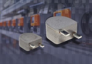
The modules are available either fully encapsulated in a compact housing or open frame. The largest module, the encapsulated MCE40, measures 3.46 × 1.50 × 1.12 inches (87.9 × 38.1 × 28.5mm) while the unencapsulated MCE03 is housed in a 1.50 × 0.65 × 0.65-inch (38.1 × 16.5 × 16.5 mm) footprint.

The MCE40 series is priced from $20.77 for 500+ units. All four MCE series come with a three-year warranty. They are available from XP Power and its authorized distributors Allied Electronics, Digi-Key, Mouser, Newark and TRC Electronics.

Power Integrations’ InnoSwitch3-EP 1,250-V GaN switcher IC extends GaN efficiency benefits to a wider range of applications.

Power Integrations has expanded its InnoSwitch family of off-line CV/CC QR flyback switcher ICs, featuring a 1,250-V PowiGaN switch. Claimed as the industry’s highest-voltage, single-switch gallium-nitride (GaN) power supply IC, the InnoSwitch3-EP 1,250-V GaN switcher IC extends the efficiency of GaN to a wider range of applications, many of which are now served using silicon-carbide (SiC) technology.

The InnoSwitch family of flyback switcher ICs feature synchronous rectification and FluxLink safety-isolated feedback. The family also offers several switch options including 725-V silicon, 1700-V SiC, and PowiGaN in 750-V, 900-V and now 1,250-V versions.

Switching losses for the 1,250-V PowiGaN technology are less than a third of silicon devices at the same voltage. This delivers power conversion efficiency as high as 93 percent for highly compact flyback power supplies that can deliver up to 85 W without a heat sink.

Designers using the new 1,250-Volt GaN switcher IC can specify an operating peak voltage of 1,000 V, enabling industry-standard 80 percent de-rating from the 1,250-V absolute maximum. This delivers headroom for industrial applications and meets challenging power grid environments.

Power Integration also offers a reference design (DER-1025) for a 60-W isolated flyback adapter that targets general use in appliances or industrial applications using a 1,250-V InnoSwitch3-EP 1250-V PowiGan switcher IC (INN3629C-H606). It is available for free download.

Pricing for the InnoSwitch3-EP 1,250-V switcher IC in the INSOP-24D package starts at $3.00 in quantities of 10,000. Samples are available and lead time for volume shipments is 16 weeks.

Microchip’s highly configurable SiC and Si SP1F and SP3F power modules are available with press-fit terminals.


Press-fit terminals provide a solder-free capability to mount power modules to a printed circuit board (PCB). Microchip Technology Inc. has announced a broad portfolio of SP1F and SP3F power modules available with press-fit terminals that address the demands of high-volume manufacturing for applications such as E-mobility, sustainability and data centers.

The solder-free, press-fit power module terminals enable automated or robotic installation that speed up the assembly process while reducing cost. The power modules combine high accuracy of the terminal locations with a press-fit design, enabling a high-reliability contact, the company said.

Using press-fit technology, power module pins are not soldered to the PCB. The connection is made by pressing the pins into properly sized PCB holes, eliminating wave soldering. This is beneficial when a PCB also houses surface-mount technology (SMT) components.

Microchip offers more than 200 variants available in its power modules portfolio. Options include the use of mSiC technology or silicon (Si) semiconductors with several topologies and ratings. The SP1F and SP3F deliver a voltage range of 600 V-1700 V and up to 280 A. The modules are fully RoHS compliant.

Press-fit terminal options are currently available.  Application note AN4322 delivers detailed mounting instructions for SP1F and SP3F press-fit use.

Infineon’s XHP 3 IGBT modules simplify paralleling and enable the downsizing of drives without sacrificing efficiency.

To meet growing demand for further downsizing and integration, Infineon Technologies AG has launched the 4.5-kV XHP 3 IGBT modules, targeting large conveyor belts, pumps, high-speed trains, locomotives, as well as commercial, construction and agricultural vehicles (CAV). The XHP family is comprised of a 450-A dual IGBT module with TRENCHSTOP IGBT4 and an emitter-controlled diode, and a 450-A double diode module with an emitter-controlled E4 diode.

The company said the new IGBT modules “will fundamentally change the landscape for medium voltage drives (MVD) and transportation applications operating at 2,000 to 3,300 V AC in 2- and 3-level topologies.”

Both modules offer improved isolation of 10.4 kV and help simplify paralleling and downsizing without sacrificing efficiency, Infineon said. “Previously, complex busbars were required to parallelize switching modules, resulting in complicated design efforts and leakage inductance.”

The new XHP family design simplifies paralleling by placing the connections side by side, resulting in the need for only a single straight busbar for paralleling.

The 4.5-kV XHP modules also reduce the number of units needed for a design. Application requirements can be reduced to two dual switches and a smaller double diode from designs that traditionally require multiple single switches and a double diode.

The combination of the XHP 3 FF450R45T3E4_B5 dual switch and the DD450S45T3E4_B5 double diode also deliver a smaller footprint and lower cost. Infineon’s previous IGBT solutions required four 140 × 190 mm² or 140 × 130 mm² switches and one 140 × 130 mm² double diode. With the new XHP family, the solution can be reduced to two 140 × 100 mm² dual switches and a 140 × 100 mm² double diode. Both modules are available now.

Onsemi adds nine new EliteSiC power integrated modules for DC ultra-fast EV chargers and energy storage systems.

Onsemi has expanded its EliteSiC power integrated modules (PIMs) with nine new devices for enabling bidirectional charging capabilities in DC ultra-fast electric vehicle (EV) chargers and energy storage systems (ESS). The EliteSiC devices are based on the company’s Gen3 M3S SiC MOSFET technology, which claims the industry’s lowest switching losses and highest efficiency.

The PIMs feature scalable output power from 25 kW to 100 kW, which enables multiple DC fast charging and energy storage systems platforms including bidirectional charging. They are available in industry-standard F1 and F2 packages with the option of a pre-applied thermal interface material (TIM) and press-fit pins.

The silicon carbide-based devices are reported to improve system cost with higher efficiency and simpler cooling mechanisms that can reduce size by up to 40% and weight by up to 52% compared to traditional silicon-based IGBT solutions. The result is smaller and lighter charging platforms to develop a “scalable network of DC fast chargers that can charge electric vehicle batteries up to 80% in as little as 15 minutes,” onsemi said.

This is significant because nearly half of U.S. consumers said the reason for not purchasing an EV is the access to charging and the ability to charge quickly, according to J.D. Power’s 2023 Electric Vehicle Consideration Study.

 The increased demand for electricity “will also put a tremendous strain on current electrical grids, potentially overloading them,” onsemi said. However, bidirectional charging is emerging as a solution to implement vehicle-to-grid, which allows for regular battery charging and the ability to use an EV as an energy storage system to power homes when needed, the company said.

 The PIM devices support key topologies such as multi-level T-type neutral point clamp (TNPC), half-bridge and full-bridge, which gives designers the flexibility to pick the right PIM for power conversion stages in their DC fast charging or ESS applications. In addition, onsemi offers advanced piecewise linear electrical circuit simulation (PLECS) models through its Self-Service PLECS model Generator and application simulation with the Elite Power Simulator, introduced earlier this year. Check out the white paper to learn more about the power converter technologies for DC fast and ultra-fast charging.

Rohm offers a new five-model portfolio of 600-V SJ MOSFETs, housed in a smaller SOT 223-3 package, saving space in power supplies, pumps and motors.

Rohm Semiconductor has added a new five-model lineup of compact 600-V Super Junction (SJ) MOSFETs, targeting small lighting power supplies, pumps and motors. The new offering of SJ MOSFETs include the R6004END4, R6003KND4, R6006KND4, R6002JND4 and R6003JND4.

Rohm explained that it has been difficult to reduce the size of the SJ MOSFETS, while maintaining an optimized balance between high breakdown voltage and low on-resistance. In response, the company developed the new models in the SOT-223-3 package (6.50 × 7.00 × 1.66 mm), which offers a smaller and lower profile form factor without sacrificing the performance of conventional products.

Compared to the conventional TO-252 package (6.60 × 10.00 × 2.30 mm), the new power MOSFETs reduce area and thickness by 31% and 27%. Rohm also noted that the same land pattern (footprint) as the TO-252 package can be used, enabling mounting on existing circuit boards without modification.

Three of the models are optimized for compact power supplies. The R6004END4 offers low noise while the R6003KND4 and R6006KND4, capable of high-speed switching, are suited for low loss and high efficiency applications. These devices target applications such as lighting, air conditioners and refrigerators.

The R6002JND4 and R6003JND4 devices use Rohm’s proprietary PrestoMOS power MOSFET technology to achieve significantly lower switching losses by speeding up reverse recovery time (trr) of the built-in diode, making them well-suited for motor-equipped devices such as pumps, fans and copiers.

The SJ MOSFETS are available through Rohm’s online distributors, including Digi-Key, Mouser and Farnell. Rohm expects to expand the family with different packages and lower on-resistance ratings.

Infineon extends its MOTIX family of MCU embedded power ICs for automotive motor control with a CAN-FD interface for faster communication.

Expanding its portfolio of MOTIX MCU embedded power ICs, Infineon Technologies AG has released the TLE988x and TLE989x bridge driver families. The MOTIX SoCs integrate a gate driver, microcontroller, communication interface and power supply on a single chip for space savings. The new families now feature CAN (FD) as the communication interface.

The MOTIX MCU TLE988x 2-phase bridge driver family and the MOTIX MCU TLE989x 3-phase bridge driver family include multiple devices with Flash memory sizes of up to 256 kB and support temperature ranges (T j max) up to 175°C. The motor driver ICs are AEC Q-100-qualified, making them suited for automotive brushed DC and brushless DC motor control applications in body, comfort and thermal-management applications. They are ISO 26262 (ASIL B) compliant.

A key feature of the bridge driver families is Infineon’s patented Adaptive MOSFET Control algorithm, which compensates for the variation of MOSFET parameters in the system by automatically adjusting the gate current to achieve the required switching. “This allows the system to be optimized in terms of EMI – electromagnetic emissions, slow slew rates – and at the same time, power dissipation – short dead times,” Infineon said.

In addition, the MOSFET control algorithm provides supply chain flexibility by maintaining the same switching behavior across variations in MOSFET production lots or differences between MOSFET suppliers, the company said.

The TLE988x and TLE989x use a B4 or B6 bridge N-channel MOSFET driver, respectively, an Arm Cortex M3 microcontroller, and a CAN (FD) controller and transceiver supporting a communication speed of 2 Mbits/s. The product families also offer about 60% more processing power compared to the TLE987x family and provide functional safety and built-in cybersecurity functions for some variants.

In addition to fast communication, these devices are reported to deliver the highest computing performance thanks to the high system frequency (60 MHz) and its dual Flash enabling read-while-write operation.

The MOTIX MCU TLE988x and TLE989x, housed in a 7 × 7-mm TQFP package, are in production. Two variants in the LQFP package with 64 pins will follow in December 2023.

For design and evaluation, the MOTIX MCU embedded power ICs offer a range of tools that include software, evaluation boards and kits, as well as several simulation, configuration and visualization tools. A 150-W coolant pump reference design is also available. In addition to sample and demo software, commercial software products cover automotive ASPICE-level-qualified motor control libraries including FOC algorithms.

Eaton extends the 9PX lithium-ion UPS line with a new 6-kVA power rating, providing remote firmware upgrades.

Eaton has expanded its 9PX lithium-ion uninterruptible power supply (UPS) with a 6-kVA power rating model, with the same capabilities of the existing 9PX lithium-ion power supplies, including remote software upgrades and integration with leading HCI and virtualization platforms. The 9PX single-phase online lithium-ion UPS family offers power ratings from 1000 – 3000 VA and is compatible with lithium-ion UPS batteries 40 percent smaller than VRLA batteries with twice the lifespan, said Eaton.

The lithium-ion UPS family delivers longer, more reliable battery backup for IT applications and is suited for edge computing environments, educational institutions, healthcare IT and light industrial.

Lithium-ion battery technology is transformative for UPSs in distributed “edge” environments, according to Eaton. The “longer battery life enables a set-it-and-forget-it approach with little on-site support from IT staff, data center professionals or maintenance personnel necessary.”

Available in tower or rack form factors, the UPS comes with the same features as the lead-acid UPS including load segments providing prioritized shutdown, remote power on (RPO), remote on/off (ROO) and output relay ports to increase control capabilities. The UPS measures 5.12 x 17.33 x 28.43 inches.

The lithium-ion battery is up to 40% lighter than lead-acid batteries and has a battery life of 8-10 years, said Eaton. Users can add up to four 2U extended battery modules for additional runtime.

The 9PX 6-kVA UPS is currently available with a 5-year warranty covering the UPS and its batteries.

Nexperia’s NPS4053 integrated 5-V load switch includes programmable current-limiting circuitry for precise control of the load current.

Nexperia has expanded its analog and logic product portfolio with the introduction of a new load switch family. The new line includes the NPS4053, an integrated 5-V load switch, which is designed with a small footprint and increased system protection.

“Load switches are essential components in the operation of a wide array of modern electronic systems,” said Nexperia. “They play a crucial role in managing current/voltage in a controlled manner from source to the load.”

Nexperia said the NPS4053 is positioned closest to the load, in a typical power chain, for power sequencing and inrush-current control and shutting off power islands to conserve power. This is a benefit in battery-operated equipment.

In addition, the load switch simplifies circuit design and has an 85% smaller PCB footprint than a comparable network of discrete components, according to the company. This makes them suited for portable devices such as notebook computers, docking stations, desktops and automotive infotainment systems.

The NPS4053 operates with an input voltage of 2.5 V-5.5 V and contains a 55-mΩ self-protected MOSFET, which manages the flow of power to the load. A key feature is the programmable current-limiting circuitry, which enables precise control of the load current over a range of 110 mA to 2.5 A with an accuracy of +6%. Other features include support for “true” reverse current blocking for end-to-end system protection and an integrated fault indicator pin that alerts the host controller of a fault event.

The NPS4053 is UL 62368 recognized and an automotive AEC-Q100 qualified version is also available. The device is offered in both leaded and leadless (HWSON 6) packages.

AOS has launched its new MRigidCSP package technology that decreases on-resistance and increases mechanical strength for MOSFETs used in battery management.

Alpha and Omega Semiconductor Limited (AOS) has unveiled its new MRigidCSP packaging technology for battery management applications. The new packaging is reported to decrease on-resistance, while increasing mechanical strength. It will be initially available for the AOCR33105E, a 12-V common-drain dual N-channel MOSFET. Target battery applications include smartphones, tablets and ultra-thin notebooks.

The MRigidCSP packaging resolves a few key challenges around fast charging, which calls for lower power loss in the battery management circuit.

“As the charging currents increase, ultra-low electrical resistance is needed for improved performance. In standard wafer-level chip scale packages (WL-CSPs), the substrate can be a significant portion of the total resistance when back-to-back MOSFETs are employed in battery management applications,” AOS explained. “A thinner substrate reduces the overall resistance but drastically reduces the package’s mechanical strength.”

AOS said the reduction in mechanical strength can result in more stress during the PCB assembly reflow, which could cause warping or cracking in the die as well as application failure.

The AOCR33105E is designed with the latest trench-power MOSFET technology in a common drain configuration. It features ultra-low on resistance and electrostatic discharge (ESD) protection to improve performance and safety in battery management, such as protection switches and mobile battery charging and discharging circuits. The device is RoHS 2.0 compliant and halogen-free. Click here for more product resources.

The AOCR33105E in the MRigidCSP package is available in production quantities with a lead time of 14-16 weeks. The device is priced at $0.405 in quantities of 1,000.